Enthone Opens Wafer Level Packaging Applications Laboratory
Laboratory will deliver customer-driven solutions to the dynamic wafer fabrication marketplace; includes electroplating processes for bump wafer, through silicon via, copper redistribution layer and copper post applications.

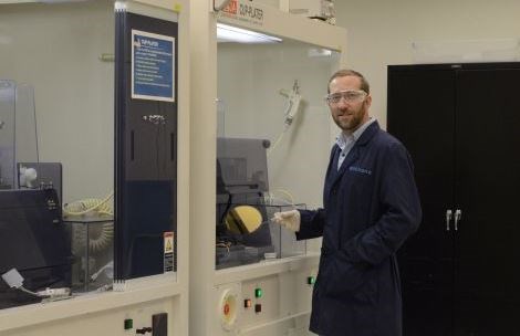
Enthone Inc. has opened its Enthone Wafer Level Packaging (WLP) Applications Laboratory. Strategically located in the heart of Silicon Valley, the mission of the Enthone WLP Applications Laboratory is to deliver customer-driven solutions to the dynamic wafer fabrication marketplace. Technologies currently being supported at the 5,000 sq. ft. facility include electroplating processes for bump wafer, through silicon via (TSV), copper redistribution layer (RDL), and copper post applications.
The Enthone WLP Applications Laboratory is staffed by the company’s electronic materials applications experts. Utilizing high-speed stir cup plating systems to simulate industry standards, the facility is equipped to perform lab scale plating and feasibility studies that demonstrate the benefits of manufacturing wafers using the company’s Microfab semiconductor packaging materials and chemistries. Sample plating and testing for process optimization, troubleshooting, bath composition analysis, and characterization of plated features and deposits for bump height, morphology, alloy composition, thin film thickness and SEM cross-sectioning for filling is also being conducted.
“The Enthone WLP Applications Laboratory provides our team of applications engineers and R&D chemists a unique opportunity to more closely collaborate with our customers and development partners, while gathering critical feedback to validate and further optimize their manufacturing process,” said Jason Maupin, Vice President Enthone Americas.
The facility will also be used to provide hands-on customer training to support their continuous improvement programs, as well as to obtain a better understanding of how Enthone chemistries may be employed for diverse applications.
Meeting the stringent requirements of the semiconductor industry, the Enthone WLP Applications Laboratory is strategically located to support some of the world’s leading semiconductor manufacturers on new and emerging technologies as they advance their product portfolio and implement higher performance, more cost-effective wafer manufacturing at their facilities throughout the globe.
The Enthone WLP Applications Laboratory is located at: Enthone, Inc., 235 Vineyard Court #150, Morgan Hill, CA 95037 USA
The Enthone WLP Applications Laboratory is managed by Brian Gokey, Enthone North America Applications Manager – WLP Manager and a Six Sigma Black Belt. Co-located with Enthone joint venture partner, Electroplating Engineers of Japan (EEJA), the laboratory is further supported by the company’s Global Development Applications Centers strategically located in Connecticut (USA), Germany, Taiwan, Singapore, and Shanghai (PRC), as well as the Alent India Research Center in Bangalore, India.
Enthone Inc., an Alent plc company, is a global and leading supplier of high performance specialty chemicals and coatings. Enthone creates customer value by providing innovative and cost-effective technology solutions to the automotive, building hardware, energy, aerospace, jewelry, industrial finishes, printed circuit board and semiconductor industries. For more information, please visit enthone.com
Related Content
-
California Public Hearing to Decide Fate of Hex Chrome Plating and Anodizing
Metal Finishing Association of California urges all members of the metal finishing community to submit comments prior to the hearing.
-
10 Anodizing Best Practices
Following this list of guidelines can help to increase the performance, cost effectiveness and quality for your anodizing operation.
-
Bryan Leiker, MFACA, Discusses CARB Public Hearing Over Calif. Hex Chrome Ban
Bryan Leiker, executive director, Metal Finishing Association of California, offers a recap of a January 27, 2023, public hearing conducted by the California Air Resources Board prior to an impending ruling on a proposed ban of hexavalent chromium use for finishing operations in the state.


.jpg;maxWidth=300;quality=90)


