Thermal Aging Effects Between Thick-Film Metallizations and Reflowed Solder Creams
Originally published as S.J. Muckett, et al., Plating and Surface Finishing, 73 (1), 44-51 (1986), this paper was awarded the 1987 AESF Gold Medal for Best Paper published in Plating and Surface Finishing in 1986. With the passage of time, Pb-containing solders have been found to have issues regarding toxicity and health. Nonetheless, the work, methodology and results discussed here remain valuable from a research standpoint.
by
S.J. Muckett, M.E. Warwick and P.E. Davis
Editor’s Note: Originally published as S.J. Muckett, et al., Plating and Surface Finishing, 73 (1), 44-51 (1986), this paper was awarded the 1987 AESF Gold Medal for Best Paper published in Plating and Surface Finishing in 1986. With the passage of time, Pb-containing solders have been found to have issues regarding toxicity and health. Nonetheless, the work, methodology and results discussed here remain valuable from a research standpoint. A printable version of this paper is available by clicking HERE.
ABSTRACT
Soldered conductor joints for hybrid microelectronic devices were examined by subjecting samples to aging at 135 or 170°C. Both tin-lead and indium-lead solders formed intermetallic compounds at the same rate over gold/platinum thick-film conductors. Over copper conductors, indium-lead solder reacted less rapidly but penetration into conductor pores was observed. A high-phosphorus brittle nickel compound was formed with both solders over a tungsten conductor with electroless nickel and electroplated gold deposits.
In the thick-film hybrid microelectronics industry, a wide range of metallized finishes can be applied on the ceramic substrate to form the circuit pattern for printed resistors, conductors and conductor lands for device attachment.1 The circuit pattern usually is produced by the screen printing of thick-film inks, which normally consist of finely divided metal powder and glass frit suspended in an organic vehicle. The thick-film substrate is then subjected to a firing regime, which burns out the organics, partially sinters the metallic particles, and allows the glass frit to fuse with the underlying ceramic layer. When high packaging density is required, a multilayer circuit may be more suitable. Such circuits can be produced by incorporating a layer of glass dielectric between successive layers of thick-film metallization.
Interconnections between thick-film conductors and discrete electronic devices are frequently made through a solder-alloy screen printed into position in the form of a paste or cream. Reflow soldering is then used to remove solvent from the cream, activate the flux, and melt the particles of solder alloy to wet the surfaces to be joined. In addition to good wetting, the metallization components must resist leaching by the solder. These factors have received considerable study, and data are available from manufacturers of thick-film inks.
For high reliability, as in military and aerospace applications, vigorous environmental and mechanical testing and the simulation of extreme service conditions are often needed to evaluate the quality and integrity of assembly components. Thermal shock, temperature cycling, thermal aging (burn-in), and vibration testing all may be carried out to some degree. The integrity of soldered joints made to thick-film conductors can be adversely affected by such conditions.2 Solid-state diffusion reactions between the solder and conductor metallization can have a deleterious effect on the adhesion of the conductor to the underlying substrate, particularly when assemblies are subjected to high temperatures for long durations.
The purpose of our study was to determine the effect of thermal aging at elevated temperatures on the solid-state diffusion reactions at the thick-film conductor/solder interface. The metallurgical reactions occurring between three solder alloys and three thick-film conductor systems considered suitable for high-reliability military and aerospace applications were investigated.
The thick-film conductors we used were selected to give a range of metallurgically different systems for study, with no intention of making specific comparisons among materials. Previously published studies aimed at quantifying the solid-state diffusion reaction rate between tin-lead solders and a number of substrates3-10 can be compared with the data in this report.
Experimental materials
Samples of a number of thick-film hybrid substrates were supplied in the as-fired condition. In each case, firing conditions were regarded as normal for the particular products in question. The systems were as follows:
- Thick-film gold/platinum (Au/Pt) and dielectric cofired on alumina.
- Nitrogen-fired, multilayer, thick-film copper and dielectric on alumina.
- Cofired, multilayer, thick-film tungsten (W) and ceramic on which nickel was deposited autocatalytically and on which gold was electroplated.
Three commercial solder creams, each formulated with a mildly activated rosin flux with 88% metal powder loading, were employed. Solder particle size and cream viscosity were chosen to allow manual dispensing by syringe on the thick-film conductors. The solder compositions were: (1) 63% tin/37% lead, with a melting point of 183°C; (2) 62% tin/36% lead/2% silver, with a melting range of 178 to 189°C and (3) 50% indium/50% lead, with a melting range of 180 to 209°C.
Each solder cream was dispensed by syringe onto rows of conductor pads of each thick-film hybrid substrate. The solder cream was reflowed using an inert fluorocarbon liquid* with a boiling temperature of 218°C in a small, laboratory-scale, vapor-phase soldering tank. Reflow time was approximately 10 sec in the primary vapor. Samples of soldered substrate were cut into coupons carrying at least one row of conductor lands wetted by each of the solder alloy compositions. The coupons were then subjected to thermal aging for up to 1200 hr in air-recirculating ovens at 135 or 170°C.
Metallographic analysis
In cross sections through soldered conductors, inter-metallic compound growth was measured optically at 1000X magnification. Each reported thickness is the mean of 40 measurements taken at different locations along the solder/conductor interface. The large standard deviations for the long aging times can be attributed to the uneven surface morphology of the thick-film conductor. Some of the thickness measurements from each sample were of an "apparent" thickness, revealed when the sectioning randomly encountered the undulating interface, thus producing an uncontrolled taper section.
Scanning electron microprobe (SEM) analysis was employed to help identify the intermetallic compounds. SEM was also used to examine the surface morphology of non-soldered conductors or, in one case, the surface of the soldered conductor after chemical stripping of the solder.
Morphological observations
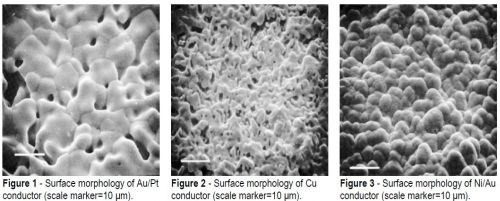
The Au/Pt conductor was approximately 25 μm thick. The surface morphology of the unsoldered material is shown in Fig. 1. No glass spheres were evident in the surface, which formed an open network of sintered fine particles. The Cu conductor was also 25 μm in thickness, and Fig. 2 shows that the metal particles were more completely sintered. However, this resulted in a porous open structure with some voids as large as 10 μm at the surface of the material. As expected, the electroplated coatings of Au (1.5 μm) and Ni (4 μm) on the thick-film W (25 μm) conductor presented a uniform closed surface (Fig. 3).
Although no pretreatment of the thick-film conductors was necessary prior to reflow soldering, defects such as non-wetting or dewetting were not observed. There were no distinguishing features between the surface morphology of solder fillets made with the tin-containing alloys, which were characteristically smooth and shiny. The surface of reflowed In-Pb solder was mat and not as smooth as the tin-based solder alloys.
The tin-based alloys showed the same structure in section except for the presence of crystals of tin-silver intermetallic compound (Ag3Sn) in the Sn-Pb-Ag alloy. Some of these Ag3Sn particles could be seen at the solder/conductor interface on the solder side of the intermetallic compound layer (Fig. 4). The sample in this SEM photograph was produced by chemically stripping the solder alloy from the surface of the conductor.
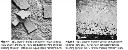
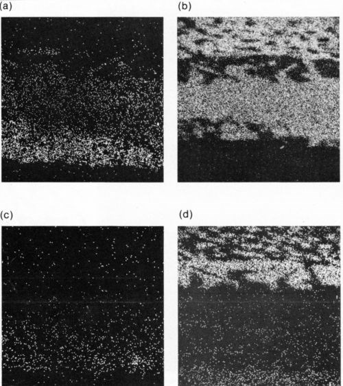
Figure 6 - X-ray images of Fig. 5: (a) Au, (b) Sn, (c) Pt and (d) Pb.
The reflow operation produced, between each of the solder alloys and substrates, layers of intermetallic compound that were consistent with the time/temperature history of the samples. Thermal aging increased the thickness of these layers, apparently without changing their chemical makeup. The Au/Pt conductor produced a layer of gold / tin intermetallic compound at the solder/ conductor interface. This compound was probably AuSn4 with both tin-based solders.
Figure 5 shows a section through such a sample after some aging, as well as the corresponding X-ray maps for Au and Sn. Figures 6(a) and (b) illustrate this increase in thickness. The Pt in the conductor does not appear to have entered the intermetallic compound region (Fig. 6(c)), and the lead-rich region in the solder next to the AuSn4 can be seen clearly (Fig. 6(d)). In the case of the In-Pb solder, the diffusion pattern on the Au-Pt conductor was similar except that the AuSn4 region was replaced by a layer of intermetallic compound identified as AuIn2.
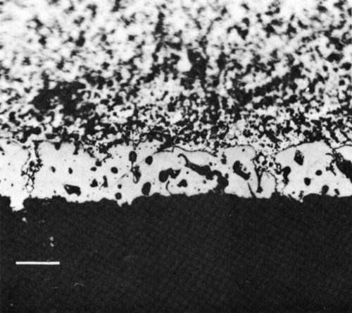
Figure 7 - Optical photomicrograph of section through reflow-soldered (63% Sn / 37% Pb) thick-film Cu conductor interface (scale marker - 20 μm).
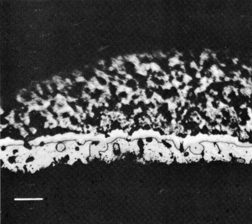
Figure 8 - Optical photomicrograph corresponding to Fig. 7 but aged for 400 hr at 135°C (scale marker = 20 μm).
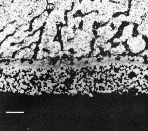
Figure 9 - Optical photomicrograph of section through reflow-soldered (63% Sn/37% Pb) thick-film Ni/Au conductor following aging at 170°C for 1200 hr (scale marker = 20 μm).
The section shown in Fig. 7 through the interface between the Cu conductor and the Sn-Pb solder in the unaged condition clearly indicates the extent of solder penetration into the open conductor structure. Thermal aging made the intermetallic compounds present at the interface more evident, and Fig. 8 shows the layers of Cu6Sn5 (white, next to the solder) and Cu3Sn (light gray, next to the conductor). Use of the Sn-Pb-Ag solder did not change the nature of the solder / conductor interface. The morphology of the system also appeared unchanged when the In-Pb solder was used but, of course, in that case the intermetallic layer was composed of an indium-copper compound, which corresponded to Cu6In5 (although this compound does not appear in the equilibrium phase diagram).
The tin-based solders both reacted with the Ni/Au conductor to produce an interface region typified by Fig. 9. This shows the tungsten thick-film layer and the continuous nickel electroplate. The thin gold electrodeposit was dissolved into the solder during reflow and was replaced by a layer of intermetallic compound, shown in greater detail in Fig. 10(a). The X-ray distribution maps for Ni, Sn and Pb in Fig. 10 (b-d) show that the intermetallic was a nickel / tin compound, identified as Ni3Sn4.
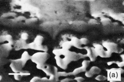
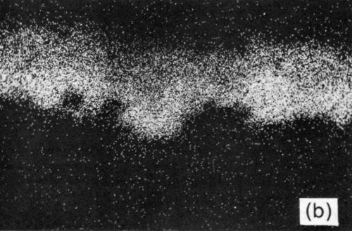
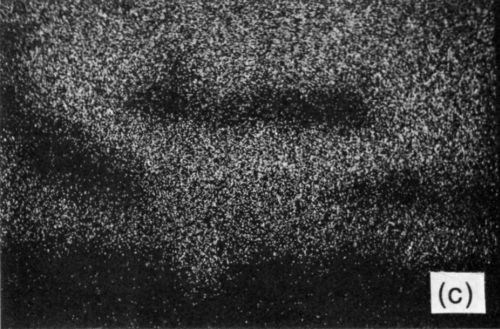
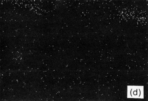
Figure 10 - (a) SEM electron image of section through Ni/Au conductor reflow-soldered (63% Sn/37% Pb) interface following aging at 135°C for 1200 hr; scale marker = 5 μm); (b) Ni X-ray image for “a”; (c) Sn X-ray image for “a”; (d) Pb X-ray image for “a”.
In the case of the In-Pb solder, the intermetallic compound layer consisted of Ni3In7, but for each of the solder alloys another interesting effect was seen. More detailed examination of the residual layer of unreacted nickel showed a high concentration of the phosphorus co-deposited during the electroless plating process and rejected from the nickel consumed in reaction with tin or indium. For example, samples soldered with In-Pb alloy and aged for 1176 hr at 170°C contained 18% P in the layer of nickel, corresponding to Ni5P2 or Ni2P with no free nickel remaining.
Growth rate of intermetallic compounds
Data on the growth rate for each conductor metallization / solder combination at 135 and 170°C were fitted to the following expressions by least-squares analysis:
x = mt + c (1)
x = kt1/2 + a (2)
where x = total thickness of the intermetallic compound layer in μm, t = time at aging temperature in hr, and m, c, k and a are constants.
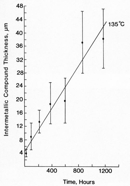
Figure 11 - Growth of intermetallic compound between Au/Pt conductor and 63% Sn/ 37% Pb solder at 135°C.
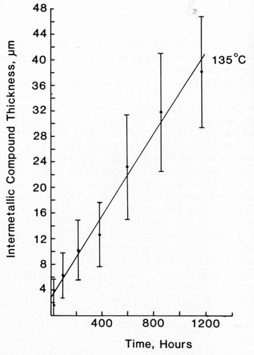
Figure 12 - Growth of intermetallic compound between Au/Pt conductor and 50% In / 50% Pb solder at 135°C.
Most of the data could be fitted equally well to both Eq. 1 and 2. In view of the large standard deviation associated with each recorded value, this is not surprising. The mathematically simpler expression (Eq. 1) was used to describe our data. Figures 11-14 plot the measured intermetallic growth as a function of time. Figure 13 also shows the effect of increased aging on the growth rate.
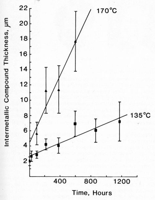
Figure 13 - Growth of intermetallic compound between Cu conductor and 63% Sn/ 37% Pb solder at 135 (■) and 170°C (▲).
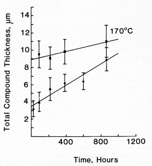
Figure 14 - Growth of intermetallic compound between Ni/Au conductor and 63% Sn/ 37% Pb solder (■) and 50% In / 50% Pb solder (▲) at 170°C.
Table 1 shows the collated growth rate data for each of the solder alloys on the Au/Pt metallization layer. Equation 1 was used to derive the experimental growth rate constant, m, and the value of c. The mean intermetallic compound layer thickness measured after reflow soldering has also been given, since this was often different from c. The results show that growth of intermetallic compound for the tin-lead solders was comparable and not affected by the presence of Ag in one of them. The growth of the indium/gold intermetallic compound layer also seemed to proceed at a rate comparable to that of the tin/gold compound. At 170°C, the metallization layer of all the systems was completely consumed long before the full aging program had been completed.
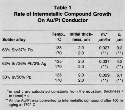
The data in Table 2 show results for the thick-film copper conductor metallization. Again, the presence of Ag in one of the tin-lead solder alloys appeared not to affect significantly the intermetallic compound growth rates. At 135°C, the In-Pb solder produced the same thickness of intermetallic as the tin-lead solders, but the acceleration in growth rate was less marked when the temperature was increased to 170°C.
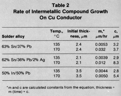
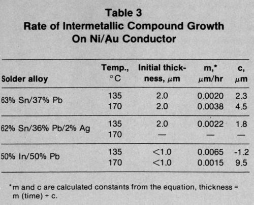
The growth rates for intermetallic compounds shown in Table 3 for the Ni/Au conductor metallization were lower than those for the other systems. The Sn-Pb-Ag solder reacted again at the same rate as the Sn-Pb solder. The In-Pb alloy produced intermetallic compound more rapidly at both 135 and 170°C.
Discussion
The interaction between Au/Pt thick-film conductors and solder alloys has been studied previously. The growth of intermetallic compound beneath In-Pb solder was described by Yost,11 who analyzed results in terms of several growth rate laws. Extended aging produced a layer identified as Au9In4, whose growth was best described by the linear law used in our study. Yost's results on aging at 130 and 160°C show good agreement with those presented in Fig. 12 and Table 1.
In a similar study, Sulouff12 described the growth of intermetallic compound layers beneath tin-containing solders on Au/Pt conductors. He preferred to relate compound layer thickness to (time)1/2, but his results were comparable with those reported here. The author also related the growth of gold / tin intermetallic compound to the loss of bond strength of the solder, and this is consistent with results describing solder joints made to electroplated gold coatings.6,7 Attempts have been made in the past to overcome the embrittling effect of gold / tin intermetallic compounds on joint strength by the addition of cadmium7 or indium14 to tin-lead solder. However, results with cadmium were erratic and the initial joint strength produced by tin-lead-indium solder was less than that given by tin-lead alloys.15 Another report16 also showed that molten 50-50 In-Pb solder dissolves gold less rapidly than tin-lead solder, suggesting that intermetallic compound growth might be similarly retarded. However, the present study demonstrates that this is not the case.
The growth of intermetallic compound layers on a copper foil substrate coated with various tin-lead alloys has been extensively reported3-5,10 for a range of temperatures. Reflowing electroplated solder coatings on a copper substrate has no effect on subsequent solid-state diffusion rates during thermal aging at 135°C.9 The compound thickness data described above were reported as a function of (time)1/2, but the actual values recorded were in good agreement with those shown in the present study. It may be concluded, therefore, that the physical form of the copper substrate does not have a significant effect on intermetallic compound growth rates, although the porous nature of the thick-film conductor surface made estimation of its thickness more difficult. Furthermore, the growth of compound within the sintered structure of the copper metallization, and the accompanying volume change, might be expected to produce problems of long-term reliability for such a system. Reducing the porosity of the copper layer would be expected to reduce the magnitude of this problem, as would limiting the penetration of the thick-film metallization by molten solder. It is ironic that in this particular case, long-term reliability might be better insured by a controlled reduction in the excellent wetting of the conductor by tin-lead alloys.
At an aging temperature of 135°C, 50-50 In-Pb solder produced the same thickness of intermetallic compound on the copper conductor as the tin-bearing solders. However, there was evidence that at 170°C, the indium-containing solder would produce less intermetallic than either of the tin alloys.
Solid nickel substrates3 and electroplated nickel finishes5 supporting coatings of various electroplated solder alloys have been thermally aged previously, and the growth of intermetallic compound layers has been quantified. The results of that work agree with the present findings for Ni/Au despite the thin layer of electroplated gold initially present on the thick-film conductor. It may therefore be assumed that when the solder creams were reflowed, the gold layer rapidly dissolved in the molten alloy and subsequently had no effect on the solid-state diffusion kinetics of intermetallic compound layer growth. This would also be consistent with the lack of an observed effect of the silver in one of the tin solders on compound layer growth.
Another factor distinguishing the Ni/Au system from nickel substrates studied previously was the presence of phosphorus in the layer of electroless Ni on the tungsten thick film. This apparently did not affect the growth of nickel/tin intermetallic compound and the phosphorus was not included in the structure of the layer. It appears to have been rejected from the compound layer, diffusing back into the unreacted nickel coating where its concentration rose. Ultimately, this diffusion would also contribute to aging of the conductor, since the nickel/phosphorus intermetallic compounds produced would be brittle and the reaction would be accompanied by a volume change. The apparent advantage of Ni/Au in terms of reduced intermetallic compound growth rates over the Au/Pt and Cu systems might not therefore be fully realized in practice. In contrast to the results of Cu metallization, the interaction between Ni/Au and 50-50 In-Pb produced a thicker intermetallic compound layer than the tin solders at both 135 and 170°C. However, the nickel/tin intermetallic contained a higher level of nickel than the compound formed with indium. Assuming the densities of each were comparable, this suggests that depletion of nickel would be at about the same rate in each case.
Conclusions
Five conclusions may be drawn from this study:
- Following reflow soldering of thick-film conductors, solid-state diffusion increases with temperature and is significant at temperatures frequently encountered during "burn-in" procedures.
- In our study, 63/37 Sn-Pb behaved in the same way as 62/36/2 Sn-Pb-Ag solder with respect to intermetallic compound growth.
- A gold/platinum thick-film conductor behaved in much the same manner as gold electroplate in producing a layer of AuSn4 and AuIn2 under tin-lead and indium-lead solders, respectively. The formation rate of these compounds was comparable.
- A copper thick-film conductor produced the same intermetallic compounds with tin-lead solder at the same rate as solid copper basis material. At the highest test temperature, indium-lead solder reacted less rapidly; but for both solders, the main observation causing concern was the penetration of the porous conductor layer by solder during reflow.
- A nickel-coated, tungsten thick-film conductor reacted with tin-lead solder as if the gold coating on top of the nickel were not present. At the same time, phosphorus present in the nickel was concentrated ahead of the advancing intermetallic compound front, producing a nickel / phosphorus compound layer. Indium-lead solder behaved in the same way as tin-lead solder.
Acknowledgments
The authors acknowledge the assistance of staff at the International Tin Research Institute and the permission of the International Tin Research Council to publish this work. Thanks are also due the British Aerospace Dynamics! Group, Hatfield Division, which supplied the fired thick-film substrate materials.
References
1. L.C. Hoffman, Ceramic Bulletin, 63, 4, 572 (1984).
2. W. Leibfried, Hybrid Circuits, 4, 19 (1984).
3. D.A. Unsworth and C.A. Mackay, Trans. Inst. Met. Fin., 51, 83 (1973).
4. P.J. Kay and C.A. Mackay, ibid., 54, 68 (1976).
5. ibid., 57, 169 (1979).
6. P.A. Ainsworth, Gold Bulletin, 4, 3, 47 (1971).
7. R. Duckett and M.L Ackroyd, Electroplating and Met. Fin., 29, 13 (May 1976).
8. P.E. Davis, M.E. Warwick and P.J. Kay, Plating & Surf. Fin., 69 (9), 72 (1982).
9. P.E. Davis, M.E. Warwick and S.J. Muckett, ibid., 70 (8), 49 (1983).
10. M.E. Warwick and S.J. Muckett, Circuit World, 9, 4, 5 (1983).
11. F.G. Yost, F.P. Ganyard and M.M. Karnowsky, Met Trans., 7A, 1141 (1976).
12. R.E. Sulouff, Proc. ISHM, 418 (1974).
13. C.J. Thwaites, Electroplating and Met. Fin., 26, 8, 10 (1973); 26, 9, 21 (1973).
14. J.D. Braun and T.B. Rhinehammer, ASM Trans., 56, 870 (1963); J.D. Braun, 57, 2, 568 (1964).
15. R. Weil, R.P. Diehl and E.C. Rinker, Plating, 52 (11),1142 (1965).
16. C.R. Jackson, Circuits Mfg., p. 40 (Jan. 1973).
About the authors (as written in 1986)

Stephen J. Muckett, formerly a research officer for the International Tin Research Institute (ITRI), recently joined Agmet, Ltd., Electroscience Laboratories, Reading, England. His work has centered principally on solders and soldering technology. Mr. Muckett graduated from University College, Cardiff, with a B.S. degree in metallurgy/geology. He then completed a one-year post-graduate course in education at Aberystwyth University, followed by two years as a physics instructor.
Malcolm E. Warwick, is head of the Metallurgy and Tinplate Division at ITRI, Fraser Rd., Greenford, Middlesex, England UB6 | 7AQ. He received his B.S. degree from Nottingham University in 1969 and his Ph.D. from London University in 1976. The division performs research on tin plating, soldering, general metallurgy, powder metallurgy, electrochemistry and other applications of tin and its alloys.
Paul E. Davis is manager of the Tin Research Institute, Inc., 2600 El Camino Real, Suite 224, Palo Alto, CA 94306. Mr. Davis received his B.S. degree in chemistry from the University of Michigan in 1950 and worked in a plating job shop before joining ITRI as a technical consultant. He spent 23 years at its Columbus, OH, facility before establishing the Palo Alto office in 1973. Mr. Davis is involved with plating of tin and tin alloys and other uses of the metal relating to electronics manufacture. He is a member of the AESF, ASTM, IPC, and the Electrochemical Society.
* Fluorinert FC70, 3M Co., St. Paul, MN.
Related Content
NASF/AESF Foundation Research Project #122: Electrochemical Approaches to Treatment of PFAS in Plating Wastewater - 12th Quarterly Report
This NASF-AESF Foundation research project report covers the 12th quarter of project work (October – December 2023) at the University of Georgia. In our previous report, we described our work on performance and effect of surface fluorinated Ti4O7 anodes on PFAS degradation in reactive electrochemical membrane (REM) mode. This quarter, our experiments involved utilizing porous Ti4O7 plates serving both as anodes and membranes. Tests compared pristine and F-18.6 Ti4O7 anodes at current densities of 10 mA/cm2 and 40 mA/cm2. This 12th quarterly report discusses the mechanisms of the effects on EO performance by anode surface fluorination.
Read MoreHexavalent-Chromium-Free Aluminum Sacrificial Paint Validation
Hexavalent chromium is a known carcinogen, repro-toxin and mutagen. Its elimination is of high importance to the aerospace industry, which has struggled to find high performing alternatives. Legacy aluminum sacrificial paints have traditionally utilized hexavalent chromium to prevent corrosion and coatings which are equal to or better than have been difficult. This second of two papers discusses the hexavalent-chromium-free process from the user point-of-view in terms of the process validation work by Rolls Royce Corporation.
Read MoreLooking Back: The Columnists
Many industrial/technical journals consist of a well-rounded mixture of technical papers, practical articles about technology and how-to-do-it features, including this one, Products Finishing. In its decades of publication, the AESF/NASF journal, Plating & Surface Finishing also endeavored to meet this need. Among the many features were those of the columnists, recognized experts who had expertise in certain segments of the surface finishing industry. This article contains a sampling of columns published in P&SF over the years, which still retain information of importance even today.
Read MoreDevelopment of a Novel Hexavalent-Chromium-Free Aluminum Sacrificial Paint
Hexavalent chromium is a known carcinogen, repro-toxin, and mutagen. Its elimination is of high importance to the aerospace industry, which has struggled to find high performing alternatives. Legacy aluminum sacrificial paints have traditionally utilized hexavalent chromium to prevent corrosion and coatings which are equal to or better than have been difficult. This first paper discusses the novel process from the supplier point-of-view.
Read MoreRead Next
Delivering Increased Benefits to Greenhouse Films
Baystar's Borstar technology is helping customers deliver better, more reliable production methods to greenhouse agriculture.
Read MoreA ‘Clean’ Agenda Offers Unique Presentations in Chicago
The 2024 Parts Cleaning Conference, co-located with the International Manufacturing Technology Show, includes presentations by several speakers who are new to the conference and topics that have not been covered in past editions of this event.
Read MoreEpisode 45: An Interview with Chandler Mancuso, MacDermid Envio Solutions
Chandler Mancuso, technical director with MacDermid Envio discusses updating your wastewater treatment system and implementing materials recycling solutions to increase efficiencies, control costs and reduce environmental impact.
Read More


