Crack Formation During Electrodeposition and Post-deposition Aging of Thin Film Coatings - 3rd Quarterly Report
Third Quarterly Report - AESF Research Project #R-118. This NASF-AESF Foundation research project report covers the third quarter of project work (July-September 2016).
by
Prof. Stanko R. Brankovic*
University of Houston
Houston, Texas, USA
Editor’s Note: This NASF-AESF Foundation research project report covers the third quarter of project work (July-September 2016) on this AESF Foundation Research project at the University of Houston. A printable PDF version is available by clicking HERE. It may be helpful to the reader to consult previous reports on this project. The links to these reports are provided at the end of this report.
Personnel:
- Stanko R. Brankovic, PI, Electrical and Computer Engineering and Chemical and Biomolecular Engineering, University of Houston,
- Kamyar Ahmadi, PhD Student, Material Science Program, University of Houston,
- Nikhil Chaudhuri, PhD Student, Material Science Program, University of Houston.
Objective:
The objective of the proposed work is to study fundamental and practical aspects of crack formation in electrodeposited thin films. The aim is to identify and quantify key parameters of the electrodeposition process affecting the crack formation in thin films. This study should enable development of an effective strategy generally applicable in practice whenever electrodeposition process for crack free films is demanded.
The activities in this period were focused on studies of electrodeposition of chromium thin films of >10 micron thickness on copper and NiCr polycrystalline substrates from Cr+3-containing electrolytes. The main experimental work involved EXDBA 1411 Bath with pH=5 (see http://short.pfonline.com/NASF16Nov2 for description).
Impedance measurements
Resistance/Impedance change of chromium films exposed to air during room temperature aging
In this period we have performed in situ impedance measurements during chromium film aging in air at room temperature and during annealing at 250°C. The experimental apparatus for in situ room temperature impedance measurements and sample configuration was already described in detail in our previous report (Report #2; http://short.pfonline.com/NASF16Dec2). The procedure for this set of experiments involved an additional step,“removal of solution,” which lasted about 3 seconds. Therefore, the samples were left to age in air while simultaneous impedance (AC resistance) transients of the chromium thin films were recorded.
The observed resistance changes for chromium films deposited with different current densities are shown in Fig. 1(a-d). The optical images of the representative morphology of the chromium surface for each sample are also shown on the right side for each transient. Impedance transients were recorded over the time intervals of 3 hr, while the approximate chromium film thickness was around 15 microns. The maximum change in the impedance value is indicated in the graph.
The common feature of all results in Fig. 1 is the quite significant magnitude of the impedance change. It ranges from 300% to 2200%. There is no obvious trend and correlation of the impedance change with respect to the conditions of the electrodeposition process and deposition current density. Initially, (Fig. 1(a-c), Fig. 2) we see the increasing impedance change with increasing current density, (j = 250-350 mA/cm2) and then, a significant decrease in relative change of impedance with further increase of current density, Fig. 1(d), and Fig. 2.
The optical inspection of the chromium samples as well as the smooth appearance of the impedance transients do indicate that no crack formation in the chromium deposited films occurs at room temperature as a result of the aging process. This is a bit surprising considering the large values of impedance change that are observed. Indirectly the data suggests that the source of such a huge change of the impedance of chromium films must be related to the increased volume concentration of the defects in the chromium films.
The important thing to notice here is a different magnitude of the impedance change for two different aging processes at room temperature. In the case of the aging of chromium films in Cr-formate solution, the change of the impedance was of the order of 1% (Fig. 2). The aging process in air, at the same temperature results in almost three orders of magnitude larger impedance change. The observed trends with respect to the current density used for sample preparation also diverge. In reality, the aging in air is the more relevant process to consider since it is to happen no matter what the application of the chromium coating might be. Yet, the huge difference in results seems to be only related to the environment (solution vs. air).
We have already discussed that the possible mechanism for creating the defects during room temperature aging of chromium films is the decomposition of CrxHy (Cr-hydride) in the bulk phase. This process can liberate the hydrogen molecules (CrxHy = 0.5YH2 + xCr) which are trapped within the bulk of the sample at the grain boundaries, or in the lattice making a gas molecules to agglomerate or create a nano-voids. They represent structural imperfections, and thus can act as electron scattering points.


Figure 1 - In situ impedance measurements of chromium films during aging at room temperature in air: chromium films deposited for ~3 hr at (a) 250 mA/cm2, (b) 300 mA/cm2, (c) 350 mA/cm2 and (d) 400 mA/cm2. Optical images are taken from the center and very near edge of the sample; AC amplitude 3 mV, frequency 50 kHz.
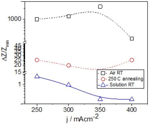
Figure 2 - Relative change of the impedance of ~15 μm chromium films during the aging process in Cr-formate solution and in air at different temperatures. Black - room temperature data from Fig. 1 (copper seed); Blue - room temperature data recorded during aging in solution (copper seed, Report #2; http://short.pfonline.com/NASF16Dec2); Red - 250°C data from Fig. 5, NiCr seed.
Hydride decomposition should also be associated with tensile stress relaxation of the films1 during aging in air at room temperature. We do observe this phenomenon as well and it is discussed latter in the report. The other possibility for increasing impedance during aging in air can be related to environmental effects and oxidation of the sample through the porous grain boundaries. Yet, we do not expect that this mechanism should be contributing to such a huge change of the impedance, as the grain boundaries of electrodeposited transition metals in general do have already segregated oxide phase.2 However, penetration of oxygen to the bulk via grain boundaries is something that can result in formation of the water phase within the film or grain boundaries. Oxygen can react with trapped hydrogen by-product of Cr-hydride degradation. This process is almost completely excluded in the case of the aging in solution as the concentration of dissolved oxygen is ~4 × 10⁻⁴M,2 a tiny fraction of the concentration of oxygen in air. Formation of water during aging in air due to an oxygen reaction with hydrogen trapped at grain boundaries, therefore, could result in formation of a different phase/medium acting as a scattering impurity for electrons, and can explain the huge difference between the two sets of data recorded at room temperature (Fig. 2). At this point, the origin of the large increase of the impedance is not explained. However, it is clear that the environment of the film makes all the difference.
Resistance change of chromium films exposed to air during annealing at 250°C
For the purpose of these measurements, we have designed a special set up where the chromium films can be controllably heated at a desired temperature and, at the same time, their impedance can be measured in situ. The initial sample geometry and preparation was the same as described in previous report (Report #2; http://short.pfonline.com/NASF16Dec2) for room temperature in situ measurements (in solution and air). The samples with NiCr seeds (100 nm) on SiO2 substrates were prepared in such a way that the conduction path in the sample was designed to go through the electrodeposited chromium film, Fig. 3(a-c). The electrodeposition set up, as in the previous measurements, was designed to match the electrode areas and separation used in the cell for in situ stress measurements, Fig. 3c. Each sample was electrodeposited just prior to the measurement to reach the thickness of ~15 microns. The chromium films were heated using a tandem of two IR heaters positioned at the back of the film, while the temperature of the film surface was measured by an IR-sensor positioned on the front side, Fig. 3d. The chromium film-fixture and the heaters were enclosed in a radiation-reflective box to minimize the heat loses to the environment. The film surface was optically accessible through the opening in the enclosure from the front side to the laser targeting mechanism of the IR sensor’s optics. This allowed precise positioning of the area/spot of the chromium film from which temperature was measured, Fig. 3(c-d). The representative temperature transient during chromium thin film annealing is shown in Fig. 4. One can see that the 250°C temperature is reached within the first 150-200 sec, and for the rest of the annealing time (3 hr), it was kept constant.
The results from the in situ impedance measurements are shown in Fig. 5(a-d). In all samples tested, the common feature of the impedance transients is a sharp decrease in the initial impedance value as the temperature is raised to 250°C, and then an increasing trend with the progression of the annealing run. All transients exhibit a sharp spikes and discontinuities which are the signature of crack formation in the chromium film. The relative change in the impedance value during the course of experiment is indicated in each transient. The representative optical images of the chromium surface are shown on the right side of the corresponding sample/transient. In some of the images, the presence of cracks is evident, although not of very high density. The films do show a slightly different surface morphology than the ones obtained during room temperature aging, Fig. 5 vs. Fig. 1. At this point however, a more quantitative analysis of the difference is not possible based on the optical images we have acquired.
The observed trend in relative impedance change as a function of the current density used for chromium deposition is quite different than the one obtained from room temperature measurements, Fig. 2. It is almost the opposite of the one observed for samples aged in air and, surprisingly, more similar to the one for samples aged in solution. The relative change of the impedance is about an order of magnitude larger than that from the samples aged in solution, and about two orders of magnitude lower than the one from the samples aged in air, Fig. 2. To some extent this is unexpected as one would anticipate that cracking of the chromium films should result in a very large increase of the chromium thin film impedance.
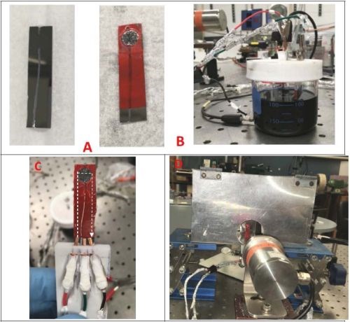
Figure 3 - The setup for in situ chromium thin film impedance measurements during the annealing process: (a) sample with patterned NiCr seed and sample with electrodeposited chromium film; (b) cell for electrodeposition; (c) sample holder during annealing with electrical connections. The current path is indicated with a white dotted line; (d) set-up for annealing displaying enclosure, sample, laser spot targeting sampling place for temperature measurement and IR sensor.
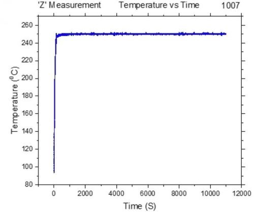
Figure 4 - Representative temperature transient during chromium thin film annealing.
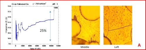


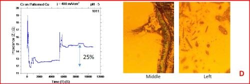
Figure 5 - In situ impedance measurements of chromium films during aging at 250°C in air. The chromium films were deposited for 3 hr at current densities of (a) 250 mA/cm2, (b) 300 mA/cm2, (c) 350 mA/cm2 and (d) 400 mA/cm2. Optical images are taken from the center and very near edge of the sample. AC amplitude = 3 mV, frequency = 50 kHz.
A closer examination of the impedance transients from Fig. 5 shows that the frequency of abrupt interrupts of the transients, i.e., chromium film cracking, is the largest for the samples deposited at 250 mA/cm2 and 400 mA/cm2 (Fig. 4a,d). The same samples do show the largest overall change in impedance. This is expected as the cracks formed do represent an ultimate obstacle for current flow. Therefore, within this experiment, the transient qualitative appearance is in agreement with the overall impedance change during annealing. The optical images of the 250 mA/cm2 sample show clear evidence of crack formation while this is not obvious in the case of 400 mA/cm2 sample.
The question still remains as to why the overall change in the impedance of the samples in these experiments is smaller than the impedance changes during room temperature aging in air. We could anticipate several possible explanations, however none of them can be confirmed at this point. They are:
(a) The formation of the cracks in the chromium films coincides with formation of the interfacial cracks between the chromium film and the NiCr seed, and therefore, the current during testing is not entirely confined with the chromium film. This could result in a large portion of the chromium films being isolated from the current flow. In this case changes in this portion of the film are not represented in the overall change of the resistance presented by the transient. The transient rather would represent the convolution of the resistance change in two current paths: seed and chromium film. Clearly in this case we deal with the artifact of the measurement and this issue needs to be resolved in the future.
(b) After the films are deposited there is a finite time passed before they are subjected to annealing experiments (one hour). In this case, their impedance is already increasing due to the aging process in air. There is the possibility that the initial decrease in the chromium film impedance during the ramping of the temperature represents the outgassing of the water we have identified as probable cause of the large change in the impedance during aging in air. Thus, annealing at 250°C represents the removal of the “impurity phase” from the chromium films, making them more homogenous from the electrical point of view. In this case, scattering from the bulk defects or second phase inhomogeneities is significantly reduced, and cracking itself then represents a much smaller portion of the impedance increase.
(c) There is one issue that still remains to be addressed in terms of complete comparability among the samples for air and annealing studies. The air experiment samples were deposited on copper seed, which is much more conductive than NiCr. Yet, copper is susceptible to oxidation, and perhaps delamination due to the aging process. Therefore, small changes in the copper seed conduction during the aging process could be the reason for the large impedance changes during aging in air. On the other hand, NiCr seed is more resistive, and adheres much better to the glass/SiO2 substrate, and we could expect that delamination does not occur, and thus the annealing experiment is less sensitive to the change in the integrity of seed itself. To resolve this issue, we plan to repeat the air aging experiments with chromium deposited on NiCr seed.
The important result is evidently the fact that the in situ impedance measurements are capable of detecting the crack formation event in the chromium film. It is still not clear if there is any critical size of the crack opening or crack length that is necessary to be manifested as a discontinuity in the in situ electrical testing. Therefore, more work and testing is necessary to fully correlate the crack formation and its detection in electrical measurements.
Stress measurements
In situ stress measurements during aging of chromium films at room temperature in air
Figure 6 shows the stress-thickness and stress-time curves for in situ measurements during deposition (250-400 mA/cm2) and subsequent aging of chromium films in air.
The three-second interruption between the deposition and aging steps of the measurements is related to the solution dispensing. The blue curves represent the stress-thickness dependence and the red curves are stress transients. The common feature of all of the measurements is that, as in the previous report, the deposition stress of the chromium films is compressive, entering a steady state mode after approximately 1.5 hr of deposition, Fig. 6(a-d).

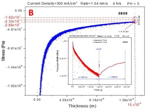

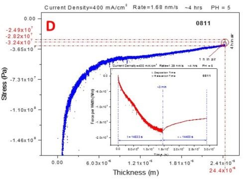
Figure 6 - In situ stress measurements during deposition (blue - transients, stress vs. thickness) of chromium films and during aging in air (red - transients, stress vs. time): (a) 250 mA/cm2, (b) 300 mA/cm2 (c) 350 mA/cm2 and (d) 400 mA/cm2.
The aging stress relaxation is tensile for each sample entering the steady state after approximately 2 hr. This behavior is very similar to what we have reported previously for the stress evolution studies of chromium films during aging in solution. The tensile stress relaxation as a function of current density used for chromium deposition has a weak decreasing trend. The magnitude of tensile stress relaxation is on the order of several tens of MPa, which is a relatively low change of stress at the end of deposition step, Fig. 6(a-d). The stress transients (red lines in Fig. 6) during deposition and aging do not show any abrupt change indicating no crack formation. This result is in perfect agreement with the qualitative shape of the in situ impedance curves shown in Fig. 1. Therefore, both in situ measurements, impedance and stress, suggest that there is no crack formation during room temperature aging of chromium films in air. This conclusion is the same as the one from our previous report where aging of chromium films in solution was studied.
Comparison between stress relaxation data for chromium films aging in air and for chromium films aging in formate solution is shown in Figure 7. Both sets of experiments yield qualitatively the same trend and the same magnitude of the stress change. To some extent this is expected, knowing that relatively more Cr-hydride per deposited chromium atom should be formed at a lower current density where the current efficiency is lower (see previous report). Assuming that Cr-hydride decomposition is the main mechanism leading to the tensile stress relaxation, we expect larger tensile relaxation for the samples deposited at lower current densities. Therefore, the agreement between stress relaxation data in these two sets of experiments shown in Fig. 7 is not surprising.

Figure 7 - The maximum tensile relaxation of chromium films during a three-hour aging in solution (red - previous report) and air (blue - data from Fig. 6).
There are two important differences between the data presented in this and the previous report. First, the tensile stress relaxation and change in impedance do not follow the same trend as a function of current density. They completely diverge, shown in Fig. 8. This is significantly different from what we have observed during the aging of chromium films in solution. In this case, the stress and impedance data agreed very well, expressing a decreasing trend (Report #2, Figs. 4 and 6).
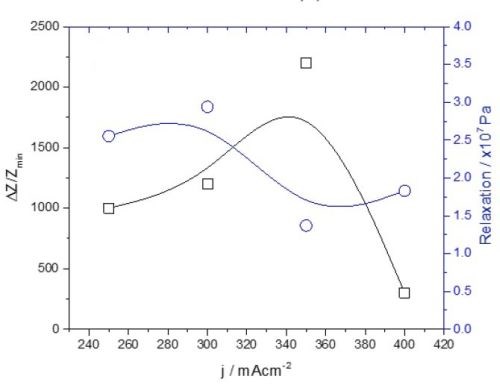
Figure 8 - Summary of the data from Fig. 1 (black lines) and Fig. 6 (blue lines).
The second important difference is the magnitude of the relative change in impedance. In the case of chromium aging in air, it is several orders of magnitude higher than for the chromium aging in solution. This has been discussed previously, comparing Figs. 1 and 5. It seems that the different environments for chromium aging, i.e., solution vs. air, do not produce significantly different stress relaxation behavior, yet they produce a completely different impedance change. This suggests that different environments do not produce significantly different structural changes or induce physical processes affecting the continuity of the chromium films and their mechanical response. It seems that the effect of environment on the aging of chromium films is mainly chemical.
Therefore, the H2O phase formation within the bulk of the film and grain boundaries, due to oxygen reacting with trapped hydrogen, a by-product of Cr-hydride decomposition, is the hypothesis that provides a plausible explanation. The other theories might also be attractive explanations, such as the oxidation of grain boundaries, etc. All hypotheses are yet to be tested. For this reason, we intend to perform additional experiments to discern the true origin of the abnormal impedance change during aging in air.
Summary
In this period, the work and measurements performed studying the chromium thin films electrodeposited from Cr+3 solution brought a new wealth of information. Experiments undoubtedly suggest that the electrical and stress measurements, in a qualitative sense, do complement each other when the main goal is to detect the crack formation in chromium coatings.
Therefore, it is likely that we will further improve these methodologies and design a more complex approach where both measurements, impedance and stress in chromium films during the aging process are performed simultaneously. This would allow us to have a 1:1 correlation between the electrical and stress evolution data. The important result that also transpires from this work is the effect of environment on chromium films impedance evolution during room temperature aging. There is strong evidence that the effect of the environment is chemical, and that the stress state in chromium films is not significantly affected. This observation has to be confirmed with more experiments with a goal of discerning if the change in the chemistry or composition of chromium films presumably induced by oxygen from the air could, at one point, affect the materials parameters of chromium films such as fracture toughness. It is clear now, that electrical testing can detect chromium cracking, which has been observed during our in situ impedance measurements during annealing at 250°C. We hope to provide more data in next report for stress relaxation during chromium films annealing which will complement these findings as well.
References
1. S.R. Brankovic, et al., Electrochimica Acta, 83, 387 (2012).
2. J. George, et al., Electrochimica Acta, 110, 411 (2013).
Past project reports
Quarter 1 (January-March 2016): Summary: NASF Report in Products Finishing; NASF Surface Technology White Papers, 81 (2), (November 2016); http://short.pfonline.com/NASF16Nov2.
Quarter 2 (April-June 2016): Summary: NASF Report in Products Finishing; NASF Surface Technology White Papers, 81 (3), (December 2016); http://short.pfonline.com/NASF16Dec2.
Footnotes:
*Corresponding author:
Dr. Stanko R. Brankovic
Associate Professor
Department of Electrical & Computer Engineering
Department of Chemical & Biomolecular Engineering
Department of Chemistry
N 308 Engineering Building 1
Houston, Texas 77204-4005
Phone: (713) 743-4409
Fax: (713) 743-4444
E-mail: srbrankovic@uh.edu
About the author

Related Content
Calculating Applied Media Force During Vibratory Finishing
What appear to be identically set-up vibratory bowls will finish identical loads of parts in varying time cycles. This paper offers a new technique to better predict what the operator will produce, by measuring the force applied to the parts. It is the efficiency of that force which controls the efficiency and speed of the refinement cycle.
Read MoreMaterial Database Enables Coating Thickness Measurement Without Calibration
The database from Coatmaster AG has calibrations of over 400 different RAL colors.
Read MoreRead Next
Episode 45: An Interview with Chandler Mancuso, MacDermid Envio Solutions
Chandler Mancuso, technical director with MacDermid Envio discusses updating your wastewater treatment system and implementing materials recycling solutions to increase efficiencies, control costs and reduce environmental impact.
Read MoreA ‘Clean’ Agenda Offers Unique Presentations in Chicago
The 2024 Parts Cleaning Conference, co-located with the International Manufacturing Technology Show, includes presentations by several speakers who are new to the conference and topics that have not been covered in past editions of this event.
Read MoreDelivering Increased Benefits to Greenhouse Films
Baystar's Borstar technology is helping customers deliver better, more reliable production methods to greenhouse agriculture.
Read More


.jpg;maxWidth=300;quality=90)


