Current Distribution on Microprofiles - The 14th William Blum Lecture - Part 3
This article is the third of four parts of a re-publication of the 14th William Blum Lecture, presented at the 60th AES Annual Convention in Cleveland, on June 18, 1973. Dr. Otto Kardos gives a comprehensive discussion of how the deposit forms on surface textures, and how leveling and brightness are achieved.
by
Otto Kardos
M&T Chemicals
Ferndale, Michigan
Recipient of the 1972 William Blum
AES Scientific Achievement Award
Editor’s Note: Originally published as Plating, 61 (4), 316-325 (1974), this article is the third of four parts of a re-publication of the 14th William Blum Lecture, presented at the 60th AES Annual Convention in Cleveland, on June 18, 1973.
A printable PDF version is available by clicking HERE.
The printable PDF version of the complete 52-page paper is available HERE.
10. Diffusion control of surface coverage as revealed by the differential capacitance of the electric double layer
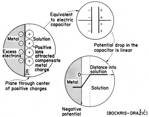
Figure 16A - The simplest imaginable electric double layer; from Bockris and Drazic.33
Like any capacitor (condenser) the electric double layer (see Fig. 16A) has a capacitance (or capacity), or for small changes of charge Q and potential E a differential capacitance C, which is given by the equation:
(30)
ΔE/Δt, and herewith C, may be obtained by superposition of AC or, less exactly, from the decay of the overpotential after current interruption.
Organic inhibitors often, but not always, decrease the capacitance of the electric double layer by displacing adsorbed water molecules, which in most cases have a greater dielectric constant than the organics.
The fractional surface coverage by the organic addition agent is given by the equation:
(31)
where C0, C and Csat are the capacitances at zero coverage, coverage Θ, and saturation coverage.
On the relation of adsorption and capacitance decrease see for instance Refs. 30, 33, 128-130. Volk and Fischer131 studied the decrease of differential capacitance produced by various nickel additives and found for uncharged compounds such as butynediol or propargyl alcohol a decrease of C0 - C with more negative cathode potential. They ascribed this change of C with E (or i) to dependence of the surface coverage by the inhibitor on the electrode potential. Balakrishnan and Fischer124 reported the decrease of capacitance produced by thiourea. Raub, Baba, Knödler and Stalzer72 used the capacitance decrease, together with the increase of overpotential and in some cases of cathodic film resistance, produced by acetylenic and other additives for their classification.
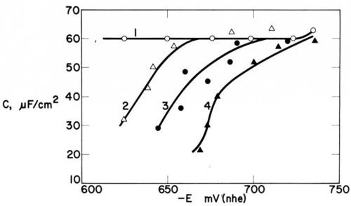
Figure 17 - Electric double layer capacitance vs. cathode potential in Watts nickel bath (30°C, pH = 4.5) (1) without addition agent at 400 to 4000 rpm and (2) with 0.2 mmol/L coumarin at 400 rpm, (3) 1540 rpm, (4) 4000 rpm; from Kruglikov, et al.100
Most relevant for the subject of this paper is the study by Kruglikov, Kudryavtsev and Sobolev.100 Figure 17 shows the decrease of differential capacitance (measured by the potential decay method) produced by 0.2 mmole/L of coumarin in a Watts nickel bath (30°C, pH = 4.5). C0 - C, and consequently from Eq. (31) surface coverage, strongly increases with the rpm of the rotating disk electrode, which indicates strong diffusion control of the surface coverage. C0 - C and surface coverage decrease with increasing cathode polarization, but - because of diffusion control revealed by the dependence of C on rpm - this decrease should, at least partly, be due to diffusion control according to Eq. (26). Figure 17 suggests that Csat is between 10 and 20 microfarad/cm2, which is confirmed by similar capacitance curves obtained with 2 mmole/L coumarin.
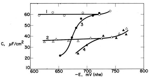
Figure 18 - Electric double layer capacitance vs. cathode potential in Watts nickel bath (30°C pH = 4.5; 1540 rpm) (1) without addition agent, (2) with 1 mmol/L p-toluenesulfonamide, (3) with 0.2 mmol/L coumarin and (4) with both addition agents; from Kruglikov, et al.100
Curve 2 in Fig. 18 shows that 1 mmole/L of the non-leveling control agent p-toluenesulfonamide lowers the double layer capacitance to about 35 pf/cm2, but in this case C0 - C, and consequently surface coverage, are constant over a wide potential and current density range, and are not influenced by a variation of the rotation rate of the disk electrode. Evidently, surface coverage by PTSA is not diffusion-controlled. Curve 4 shows the synergism of the two addition agents.
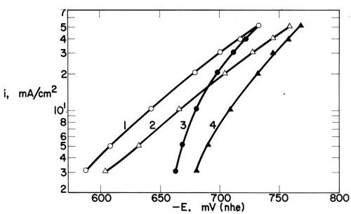
Figure 19 - Polarization curves in Watts nickel bath (30ºC, pH = 4.5, 1540 rpm); (1) without addition agent, (2) with 1 mmol/L p-toluenesulfonamide, (3) with 0.2 mmol/L coumarin, and (4) with both addition agents; from Kruglikov, et al.100
Figure 19 shows the corresponding polarization curves. The extra polarization (-ΔE) produced by the additives is closely related to the decrease of capacitance, C0 - C, produced by them, and to the corresponding surface coverage. For the diffusion-controlled coumarin, -ΔE, just like C0 - C and Θ, strongly increases with decreasing current density (as predicted by Eq. 26). For the not diffusion-controlled PTSA, -ΔE, C0 - C, and Θ are constant over a very wide potential and current density range. The correspondence between -ΔE and C0 - C produced by various additives was also shown by Volk and Fischer.131
11. The disappearance of diffusion control with some types of interrupted current
In linear diffusion, that is diffusion to a flat electrode, the thickness of the diffusion layer would continuously increase with time if convection were absent. In the presence of convection, however, the diffusion layer reaches its steady state thickness in a few seconds after switch-on of the current. See e.g., Ref. 33, p. 134. After interruption of the current, the concentration of the consumed species in the diffusion layer is replenished by diffusion. The decay time of the diffusion layer is several times longer than its formation time and decreases with increasing agitation.98,101,132 If, after the decay of the diffusion layer, the current is switched on again (e.g., at 4 A/dm2) the initial overpotential in a coumarin-containing nickel bath may be more negative than its steady state value by as much as 150 mV.98,101,132 At high coumarin concentration and low current density (0.5 g/L, 0.1 A/dm2), where diffusion control is absent (CE CB), no such initial excess overpotential occurs.98
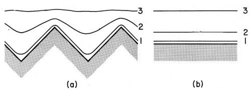
Figure 19A - Schematic comparison between nonstationary diffusion on (a) a rough homogeneous surface and (b) a flat homogeneous surface. Lines 1, 2 and 3 indicate equiconcentration planes for times t1 < t2 < t3. From DeLevie.36
It should be kept in mind that over a microprofile the diffusion layer boundary is, for the fraction of a second after the current switch-on, very close and parallel to the profile contour.12,36,133,134,178 Then the diffusion layer boundary gradually recedes and flattens and its local thickness varies more and more until after a few seconds the steady state is reached; (Fig. 19A). The length of the time after current switch-on during which the diffusion layer thickness is practically uniform over a microprofile strongly decreases with decreasing profile size.
One would thus expect a decrease of leveling if, with periodically interrupted current, the cathodic electrolysis time during each cycle, te, is not long enough to produce the maximum nonuniformity of δ over the profile, and if the interruption time, ti, is sufficiently long to destroy the incipient diffusion layer formed during the preceding pulse. If te is so short that the diffusion layer thickness is still uniform over the profile, and ti long enough to destroy this very thin diffusion layer, all leveling, except, of course, geometric leveling, should disappear. Exactly this is shown in Fig. 20, obtained by Kruglikov, Kudryavtsev and co-workers101 (compare also Refs. 98 and 132) which plots the percentage of leveling in a coumarin-containing nickel bath against the pulsation frequency. Leveling was determined on V-shaped microgrooves on the rotating disk electrode, initially 50 μm deep, with an included angle of 60°. Deposit thickness on the flat area was 4 μm. The Watts nickel bath (30°C, pH = 4.5) was saturated with coumarin. With te/ti = 1/4 (curve 2), when the frequency becomes greater than about 0.1 cycle/sec or te becomes smaller than 2 sec, leveling begins to decrease. At a frequency equal to 1 cycle/sec or te equal to 0.2 sec most leveling disappears, and at a frequency of 10 cycles/sec or te equal to 0.02 sec all leveling, except geometric leveling, has disappeared. It should be noted that the critical frequencies for the disappearance of leveling, and diffusion control in general, on 100 times less deep grooves (0.5 μm) should be 10,000 times greater, because of the proportionality of diffusion layer thickness to or 1/
.133
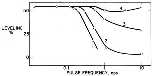
Figure 20 - Leveling vs. pulse frequency in nickel bath (30°C, pH = 4.5, 4 A/dm2, 430 rpm) saturated with coumarin; initial groove depth 50 μm, notch angle 60°, deposit thickness on flat surface 4 μm. Electrolysis time/interruption time = (1) 1/12, (2) 1/4, (3) 1/1, (4) 3/2. From Kruglikov, et al.101
The 50% leveling shown in Fig. 20, obtained on an initial groove depth of 50 μm thickness (on flat), is quite substantial and corresponds to a h3/h1 ratio (see Fig. 7) of more than 7.98,132
If te/ti is too great (e.g., 3/2 in curve 4), then the diffusion layer developed during a pulse is only partly destroyed during the following interruption time and thus its thickness increases during each cycle until it reaches its normal value. Consequently, leveling is scarcely diminished.
Figure 20 is a very strong proof of the diffusion mechanism of leveling in coumarin-containing nickel baths, at least on grooves of the examined depth (30 and 50 μm). It is difficult to imagine that other leveling mechanisms such as the shape-sensitive adsorption suggested by Thomas5 or the cyclic mechanism of Zak179 would show a similar dependency on pulse frequency.
If the pulse time is short enough, and the interruption time sufficient to destroy the rudimentary diffusion layer formed in the preceding pulse, also the unfavorable influence of rate control by the mass transport of the depositing metal ions should disappear. Thus "bad microthrow," increase of original surface roughness, formation of dendrites and metal powder can be avoided.133,134,178 See also Ref. 133A on the induction time required for the appearance of diffusion controlled amplification of surface roughness.
While the diffusion layer thicknesses obtained in electroplating are generally between 20 and 200 μm, and most intense mechanical agitation may reduce it to 0.8 μm, Braun and Ibl134,178 obtained with pulse times of 0.7 to 30 microseconds (μsec) diffusion layer thicknesses of only 0.025 to 0.2 μm. The boundaries of such thin diffusion layers can follow the contours of even very fine surface roughness and are smaller than the radius of the finest dendrite tips. Consequently, diffusion-controlled roughening of the metal surface is avoided, even at a current density as high as 25,000 A/dm2 during the cathodic pulse and an average current density during the cycle of 37.5 A/dm2, in an acid copper bath flowing at a velocity of 2 m/sec. A similar effect is obtained with high-frequency (e.g., 10,000 cycles/sec) pulsation of the cathode potential.133
With a uniform diffusion layer thickness over the microprofile, electrodeposition at the limiting current density even improves the uniformity of metal deposition and concentration polarization throws the deposit into the microrecess just as it does on macrorecesses.l34,178
Interrupted current of a more usual type (e.g., te = 3 sec, ti = 12 sec, iav = 3 A/dm2) reduces roughness formation in acid copper baths.177 Various cycles of interrupted current are useful in industrial cyanide plating where they reduce roughness formation and improve microthrow, especially in the high current density range.
12. Quantitative prediction of leveling
Idle arguments for a diffusion theory of leveling assembled in the preceding sections are many and seem to be very strong. They seem to explain the general features and trends of metal deposition on microprofiles. It is thus surprising that very few attempts were made to predict or explain quantitatively the thickness ratios obtained in a microgroove of a specific shape and under specific conditions. Such attempts were made by Gladshtein and Kadaner135 and were apparently quite successful, as far as I can judge from my unreliable translation of the Russian original and from the short abstracts in English.136 These authors predicted thickness ratios on a V-shaped groove (β = 60°, depth = 0.25 mm) and a rectangular groove (0.1 mm deep and wide) from a coumarin-containing nickel bath, for instance, by the following method: They made models of the two grooves on semiconductive paper, on which they determined the primary current distribution ratios (in/i10)pr for the 10 equal sections of the grooves, sections 8 to 10 being situated on the flat surface. Because of the analogy of limiting diffusion flow and primary current distribution jLn/jL10 = (in/i10)pr. From Eq. (15) they obtained the "equivalent" coumarin concentrations Cn/C10 = jLn/ jL10 and, combining these two equations, Cn/C10 = (in/i10)pr. From polarization measurements they predicted the local current density on each groove section corresponding to the local "equivalent" coumarin concentration at the electrode potential required to give the selected current density at section 10. The predicted and the actually measured current density and thickness ratios agreed remarkably well. This success should encourage similar attempts at quantitative prediction of deposit thickness ratios on microprofiles.
The influence of the microprofile shape on microthrow and leveling is easily predictable: As well on isolated V-grooves as on triangular wave profiles increase of the enclosed angle (notch angle) β makes primary current distribution and thus diffusion flow at constant CE more uniform.29 Consequently bad microthrow, e.g., from cyanide baths or from acid copper baths at high current densities, improves with increasing β, or as tan (β/2) = (width/2 × depth) with increasing width/depth ratio. On the other hand, true leveling, and from Fig. 2 also geometric leveling, decrease with increasing notch angle. These expectations were confirmed by Raub,45 Müller and Raub45A and Cheh,160 and on trapezoidal grooves by Sundarayan, Rayagopalan and Reddy.138
A triangular wave profile should give a greater variation of jL, and δN, than V-grooves of the same notch angle β. This seems to agree with DuRose's78 finding that less coumarin is required for maximum leveling on satin surfaces than on isolated notches.
Overplating should be avoided to minimize the influence of geometric leveling.45A If one wishes to study the influence of groove size on leveling, it is therefore recommended to decrease deposit thickness in proportion to groove depth.
13. A new and completely different leveling mechanism
Until recently, only two main cathodic leveling mechanisms were known: diffusion-controlled inhibition producing "true leveling" and uniform current distribution producing "geometric leveling." A less frequent mechanism was described by Sundarayan and co-workers.138 They obtained moderate leveling in trapezoidal grooves from a cyanide copper bath containing no additives at high rotation rates of the cylindrical cathode. They ascribed this to turbulent flow within the grooves leading to increased supply of the complexed metal ions.
But in fall 1972 Professor Ibl sent me a copy of the doctoral thesis of Dr. Ing. J. Schulz-Harder107 in which the latter described a completely new and different leveling mechanism. Schulz-Harder obtained substantial leveling by predipping or preplating an electroformed copper panel containing V-shaped grooves (30 μm deep) in an acid copper bath containing 60 mg/L sodium chloride, a polarizing control agent, PCA, and a depolarizing control agent, DCA, similar to, but not identical with, those we had used in the experiments leading to our Fig. 13 and Table 2, rinsing it in an acid copper bath containing no additives, and finally plating it in a copper bath containing only chloride and PCA.
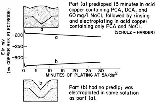
Figure 21 - Copper deposits on microgrooves (30 μm initial depth) and cathode potentials (at 5 A/dm2) from non-leveling acid copper bath (a) with activating predip and (b) without predip; replotted from Schulz-Harder.107
The upper photomicrograph in Fig. 21 shows the copper deposit obtained after 13 min predip in the PCA + DCA + Cl- bath (similar to solution No. 5 in Table 2), followed by rinsing and final plating (32 min at 5 A/dm2) in the PCA + CP bath free of DCA (similar to solution No. 3). It shows strong leveling and even "superleveling" because of the hump formation over the groove. The lower photomicrograph b in Fig. 21 shows the non-leveling copper deposit obtained in the PCA + Cl- bath without predip. The graph shows the cathode potentials (against a copper wire) during the plating of deposit (a) after predip and deposit (b) without predip. The preceding predip, although followed by a rinse, depolarizes copper deposition by about 150 mV, just as the addition of 15 mg/L DCA to a copper bath containing 60 mg/L Cl- and 1 g/L of a PCA depolarized by 163 mV (Experiment No. 5 vs. 3 in Table 2). (It should be noted that the cathode potentials of Fig. 21 are measured against a copper wire and are consequently much less negative than those given in Table 2 for similar additives against the saturated mercurous sulfate electrode.) The copper surface thus shows a "memory" for the pretreatment which only slightly decreases during the 32 min plating time.

Figure 22 - Copper deposits in dependence on plating time after activating predip as in Fig. 21A; from Schulz-Harder.107
Figure 22 shows successive deposit thicknesses obtained after predip under the same conditions as Fig. 21A.
Schulz-Harder's interesting explanation of these phenomena is based on a fact and a hypothesis. The fact is that uniform metal deposition reduces the surface area over a microgroove, increases it over a micropeak, and leaves it unchanged over a flat area. The hypothesis is that the "catalyst" (stimulator, depolarizer) DCA is relatively slowly adsorbed and still more slowly incorporated or desorbed. During the predip the copper surface becomes evenly but not completely covered by DCA, but during the following plating the surface area over the groove bottom shrinks and consequently ends up with a higher surface coverage by DCA and thus will grow faster than the other areas. The opposite happens over micropeaks or convex surface areas. This hypothesis assumes that the copper grows below the adsorbed catalyst and "pushes it up" or "carries it along" while growing.
Preplating (8 min) in the PCA + DCA + Cl- bath No. 5 followed by rinsing and plating (24 min) in the PCA + Cl- bath No. 3 gives results similar to those described in Figs. 21 and 22. For some other DCA compounds only the preplating and not the predip method produces leveling.
Also a predip (5 min) in the acid copper bath No. 4 containing chloride + PCA + only 10% of the regular DCA concentration followed by plating (32 min at 5 A/dm2) in the same bath gives moderate leveling. We confirmed this on a scratched Hull Cell panel and also found that the predip is not required. However, in both cases the leveling is considerably lower than can be obtained in the presence of a typical leveling agent, that is, a diffusion-controlled inhibitor.
Concentrations of the catalyst DCA in predip, preplating solution and, with the just described procedure, in the plating bath itself, and predip or preplate time are somewhat critical. If surface coverage is at or near saturation on all profile points, then shrinkage of the surface area in the groove cannot produce any, or at least not much, increase of the surface coverage by the catalyst and of the metal deposition rate.
This new "surface controlled catalysis" mechanism of leveling, discovered by Schulz-Harder, is bound to attract considerable attention as soon as it becomes more widely known. It should strongly contribute to the understanding of addition agent action, but it seems that in strongly leveling industrial plating processes the presence of diffusion-controlled inhibitors, that is of the regular type of levelers, will continue to be indispensable.
The "memory effect" discovered by Schulz-Harder is remarkably long-lasting. It brings to mind other memory effects such as the influence of the substrate structure on the deposit structure, the persistence of fingerprints on the substrate even through fairly thick electrodeposits if cleaning is insufficient, and the preplate influence described by Edwards64 and Edwards and Levett.67 These authors showed that a preplate in a nickel bath containing inactive saccharin and either succinonitrile or quinoline methiodide, followed by a rinse, increases subsequent codeposition of sulfur from a nickel bath containing radioactively labeled saccharin. They ascribed this effect to the creation of adsorption sites (or could they be reduction sites?) for saccharin in the preplate bath containing the mentioned additives (but not in a preplate bath containing, e.g., only inactive saccharin). This memory effect fades rather quickly; after 2.5 sec plating in the second bath, it decreased to less than one third of the magnitude it had at only 0.5 sec plating time.
A predip effect observed by Vagramyan and Baraboshkina141 will be discussed in Section 14.
The "pushing up" or the "carrying along" of the adsorbate by the growing metal deposit required by Schulz-Harder's leveling mechanism (unless the latter is explainable by the creation of especially active growth sites) could have some relation to the formation of laminations. The replica electron micrographs and especially the transmission electron micrographs of thin foils of a proprietary bright nickel deposit, obtained with a special technique by Weil and Jacobus,143 reveal a finer grain structure of the lamination boundaries ("dark bands" developed by electropolishing or etching) which the authors relate to periodic fluctuation of the concentration of adsorbed or codeposited additives. Could it be that "some or all" of the adsorbed additives are "pushed up" until at a critical surface concentration of "some or all" they are incorporated? The situation becomes especially interesting and complex because all proprietary bright nickel baths contain control agents (see DuRose's definition41) such as aromatic or otherwise unsaturated sulfonates and sulfonamides which require splitting of the C-S bond by hydrogenolysis41,113-115 before sulfur (and sometimes also carbon120) is codeposited and, on the other hand, leveling brighteners which become less adsorbable by hydrogenation.66,68,105,106,109,113-115 What is then "pushed up": only the control agents or also the leveling brighteners? Do the dark bands contain only more codeposited sulfur or also more codeposited carbons? Compare also the related papers by Weil and co-workers.142,144,145
14. Brightening
The brightness of a surface is related to the practical absence of surface roughness of the order of the wavelengths of light, namely 0.4 to 0.8 μm for violet and red light, respectively.
Weil and Paquin139 showed that the eye evaluation of the brightness of various nickel deposits corresponds to the percentage of specular reflection (angle of reflection = angle of incidence) of light from them and to the fraction of surface area free of roughness of 0.15 μm or more depth. The following equation shows the dependence of the ratio of diffuse reflection (Rd) to total reflection (Rt) on the RMS roughness of the surface (σ) and the wavelength of light (λ):140
(31A)
To get a high degree of brightness, that is, a low Rd/Rt, the RMS roughness of the surface should thus be substantially smaller than the wavelengths of light.
It is important to distinguish between brightening of a matte surface and brightness maintenance, that is, suppression of roughness formation on an originally bright substrate. Both effects were studied by Vagramyan and Baraboshkina.141 With the help of a specially designed instrument, including a photocell, they measured specular reflection from nickel deposits during plating in a variety of nickel baths. They used two substrates: matte nickel and bright nickel. Most crystallites on the former were four-sided pyramids of 0.7-1.0 μm width and with valleys between them of an average depth of 0.3-0.4 μm. The surface of the bright nickel, deposited from a Watts nickel bath containing 0.3 g/L thiourea, appeared smooth even at 16,000× magnification.
Figures 23 to 25 show the dependence of reflectivity (expressed as microamperes flowing through the photo-cell) on deposit thickness. Standard conditions were 40°C, pH = 4.0, 4 A/dm2, no agitation, in a well-purified Watts nickel bath.
The ascending curve in Fig. 23 shows the rapid increase of the reflectivity of the matte nickel substrate in nickel baths containing the leveling brighteners butynediol (1 g/L) or thiourea (0.3 g/L). With about 3 μm deposit thickness, full brightness is reached. The upper curve shows the excellent brightness maintenance during plating on a bright substrate. In absence of additives, the reflectivity would fall until the initial value of the ascending curve is reached with about 12 μm deposit thickness.
Figure 24, obtained in presence of 1 g/L coumarin, shows the rapid increase and decrease, respectively, of brightness to the semibright level which is characteristic for deposits from a coumarin-containing bath. Compare also the interesting electron micrographs of Weil and Cook.142
Figure 25, obtained in presence of 2 g/L saccharin, shows a much slower rate of brightness increase to a semibright level but a rather good brightness maintenance.
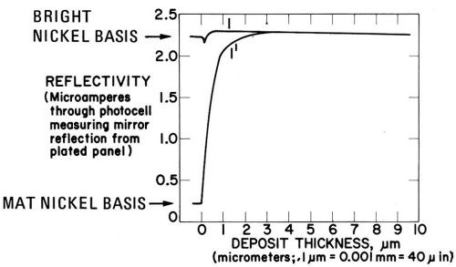
Figure 23 - Change of specular reflection with nickel deposit thickness on bright nickel substrate (1) and mat nickel substrate (V). Watts nickel bath (40 C, pH = 4.0, 4 A/dm2, no agitation) containing 0.3 gL thiourea or 1 g/L butynediol; from Vagramyan and Baraboshkina.141
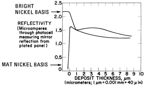
Figure 24 - As Fig. 23 but with 1 g/L coumarin as the addition agent.141
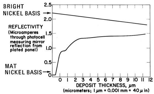
Figure 25 - As Fig. 23 but with 2 g/L saccharin as the addition agent.141
How does one interpret these results, especially those referring to the brightening of matte substrates, which is obviously a smoothening or leveling process? To compare the rate of leveling over a microgroove 0.35 μm deep and over another one 25 μm deep one should keep deposit thicknesses proportional to the groove depths. The 100% leveling obtained in Fig. 23 on a 0.35 μm roughness with 3 μm deposit would require a 70 times thicker deposit, that is 210 μm, for the 25 μm deep groove. Apparently, the rate of leveling over the matte nickel is of the right order, but somewhat smaller than expected. This applies also to the apparently geometric leveling in Fig. 25 and may perhaps be due to the absence of agitation. Evidently, a much more detailed and quantitative comparison would be desirable.
Vagramyan and Baraboshkina bring two arguments against the existence of a diffusion-controlled leveling mechanism on such fine profiles. First they argue that with a roughness of, e.g., 0.3 μm, and a diffusion layer thickness of, e.g., 140 μm, the diffusion layer thicknesses over micropeak and microrecess would be 140 μm and 140.3 μm, respectively, and thus δr/δp 1. This is correct as far as it goes but the ratio of limiting diffusion rates jLp/jLr is equal to the ratio of the effective or equivalent diffusion layer thicknesses δNr/δNp, which remains unchanged if the profile size is reduced, just as primary current distribution is independent of profile size or of the distance of the anode if the latter is sufficiently far away. This is because a micropeak receives more diffusion flow not only because it is nearer - and in the case of very fine-scale roughness, just a trifle nearer - to the diffusion layer boundary, but mainly because it diverts diffusion flow toward itself by being accessible from several directions.146
Vagramyan and Baraboshkina's second argument against diffusion control on very fine-scale roughness and for "specific" or "shape-sensitive" adsorption in the sense of Thomas5 or Beacom and Riley116,117 is based on the following experiment: they dipped a still active matte nickel deposit in an aqueous thiourea solution, rinsed it in distilled water, and obtained leveling during subsequent plating in a nickel bath containing no additives. This "memory effect" (see Section 13) seemed to indicate "selective" or "specific" adsorption, instead of diffusion-controlled adsorption, on the micropeaks. Their experiment requires further analysis. Immediately after the immersion of the matte nickel into the thiourea solution, there would be no diffusion layer present. Then a diffusion layer would form, first of equal thickness, then of unequal thickness over the profile. Finally, after the surface becomes saturated with thiourea or one of its reaction products with nickel hydride, namely nickel sulfide,61 the diffusion layer would decay. It would, consequently, be important to know which stage was reached in the predip. Furthermore, considering the depolarizing or stimulating effect of thiourea at certain concentrations, or at very low current density even at all concentrations,3 one could wonder whether the leveling obtained after the predip would not be of the Schulz-Harder type described in Section 13.
The experiments reported in Section 948,60,70,121,122 show conclusively that the overall adsorption and consumption rate of thiourea in nickel baths is, during the "steady state" of nickel plating reached after a few seconds, diffusion controlled. That means that peaks, valleys, flats will adsorb and "consume" all the thiourea molecules arriving at the limiting diffusion rate, and consequently more on micropeaks than on microrecesses, unless it can be proved that the difference of limiting diffusion rates to micropeaks and microrecesses disappears on very fine-scale profiles. Vagramyan and Baraboshkina's first argument did not seem to prove this and the presently available experimental data seem to disprove it. One may cite here Watson and Edwards's finding3 that maximum leveling is obtained at about the same coumarin concentration whether the microgrooves are 20 μm or 0.1 μm deep (see Section 3) and the prevention of roughness formation at high current density with interrupted current133,134,178 which was shortly discussed in Section 11.
Thus, my peace of mind was not disturbed until I received a letter from Dr. Schulz-Harder, dated January 31, 1973. I would like to translate some of the significant passages in this letter from the original German:
"First I would like to express my opinion concerning your thesis that the diffusion-controlled inhibitor mechanism applies also to roughnesses the dimensions of which are very small, e.g., in comparison with Nernst's diffusion layer thickness. This assumption is correct if the inhibitor consumption occurs on all points of the surface at the limiting rate and consequently the concentration of the inhibitor in vicinity of the surface becomes zero. This concept applies only in rough approximation. In reality surface concentrations" (this applies obviously to CE and Θ of this paper) "must be different to make leveling possible . . .
"In this case there exists a characteristic length LD, which indicates the order of the profile dimensions, from which on substantial decrease of these dimensions produces no more difference in the surface concentrations of the inhibitor and consequently no more leveling."
This parameter LD is similar to Wagner's polarization parameter kc and Schulz-Harder calculates it as (if we use some of the symbols of this paper):
(32)
where kº is a complex reaction constant calculated from the adsorption, desorption, and consumption rate constants of the inhibitor. (These ideas were developed by Dr. Schulz-Harder in cooperation with Professor Dr. J. Osterwald).
If reversible (unchanged) desorption can be neglected and surface coverage is far from saturation, kº is equal to kads (see Eq. 24). Then an equation similar to (8), but for adsorption rates instead of current densities, results:*
(33)
*From ,
, and the simplification,
If d/sin (β/2) - and consequently the smaller groove depth d itself - is substantially smaller than D/kads, adsorption rates should become practically uniform unless, of course, kads varies over the profile and is e.g., greater on micropeaks. However, the critical adsorption or diffusion parameter LD = D/kads decreases with increasing kads. As shown in Section 6, kads >> kT is characteristic of strict diffusion control. Diffusion-controlled inhibition (or stimulation) should thus exist down to very fine profile sizes if kads is sufficiently large.
Consideration of the inhibitor diffusion from micropeak to microrecess, which reduces adsorption on the peak and increases it on the recess, leads to a similar conclusion (Compare Section 2). This diffusion rate is equal to D(Cp - Cr)/s, where s is the length of the groove side. To obtain jads p/jads r 4, one would need Cp/Cr
4 (if the influence of a variation of θ can be neglected; see Eq. 24.). But the resulting diffusion flow from peak to recess is, of course, 10 times smaller with Cp = 0.004CB and Cr = 0.001CB than with Cp = 0.04CB and Cr = 0.01CB.
Similar considerations apply to metal deposition in absence of inhibitors, where Cp and Cr would refer to the metal ion concentrations. In this case, transport-controlled roughness increase of the very fine initial roughness is so well-proven12,133,134,155,156,178 that strict transport control must exist down to a very fine scale of roughness.
Now to roughness formation and its suppression by inhibitors, or "brightness maintenance."
In absence of mass transport control, roughness develops on polycrystalline substrates because of the different growth rates of crystallites of different orientation147,148 and on single crystals, or on the individual crystallites of a polycrystalline surface, by the bunching of monoatomic layers to polyatomic layers ("macro-steps"), the development of ridges, growth spirals, pyramids, blocks, etc., by mechanisms discussed in Refs. 33, 88, 89, 90, 140, 147-154.
Transport control strongly increases the rate of roughening because, except with pulsed current or potential of sufficiently high frequency or of sufficiently short cathodic pulses and sufficiently long rest periods,133,134,178 the diffusion layer thickness is smaller over the micropeaks than over the microvalleys. This diffusion-controlled roughness formation was studied especially by Ibl and associates48,56,134,155,156,178 and was recently surveyed by Despic and Popov.12,133,133A
A special case of diffusion-controlled roughness formation is dendritic (tree-like) growth. According to the theory initiated by Barton and Bockris157 and further developed in Refs. 158 and 159, a growth spiral or pyramid becomes, after the required induction time,133A tall and steep under diffusion control until it penetrates the diffusion layer characteristic of the substrate. Then linear diffusion is replaced by spherical diffusion and Eq. (16) is replaced by the corresponding equation for spherical diffusion
(34)
where r is the radius of curvature of the dendrite tip. If r is much smaller than the diffusion layer thickness of the substrate, the dendrite will grow at a much faster rate than the rest of the surface. See also Refs. 12, 33, 89.
How do inhibitors suppress roughness formation? Hoar161 suggested that the production of a bright surface (other than by mechanical means) involves the deposition, or in the anodic case removal, of surface atoms in a random manner. He proposed two mechanisms by which equalization of the growth rates on different crystal planes and consequently brightening would occur (compare Ref. 88). One mechanism is due to nearly complete surface coverage by an additive which is reversibly adsorbed and desorbed; metal deposition would then occur through the randomly forming holes in this adsorbed film and would consequently be uniform. The other mechanism consists in preferred adsorption of the inhibitor on the more active faces or growth sites, which would also lead to an equalization of the local deposition rates. DuRose78 has placed nickel brighteners in one of these two groups, or in an intermediate group, according to their adsorption and inhibition mechanism.
Some growth sites, which are generally more active than others but need not be so, are especially sensitive to adsorbed inhibitors in respect to the change of crystal structure and surface roughness. This applies especially to screw dislocations,153 including the emerging screw dislocation (or group of dislocations) which operates at the apex of a pyramid.90,162
Could a diffusion-controlled inhibition mechanism contribute to brightness maintenance? Perhaps in the case of the leveling brighteners butynediol, thiourea, coumarin (Figs. 23 and 24) but not with saccharin (Fig. 25) which gives no leveling, except geometric leveling, and shows at 2 g/L no signs of diffusion-controlled inhibition or consumption on flat surfaces.
Epelboin, Froment and Wiart164 measured by differential interferometry the maximum amplitude, eM, of the microprofile formed by plating 10 μm of nickel on an initially smooth rotating disk electrode from nickel baths containing butynediol. They found 1/eM and consequently brightness strongly increasing with until a plateau was reached at eM equal to about 0.02 μm for 0.6 to 2 mmoles/L butynediol, but higher plateaus for smaller concentrations. Thus, brightness maintenance by butynediol shows certainly signs of diffusion control but it is questionable whether this diffusion control applies only to the overall surface coverage or also to the greater coverage on incipient very fine micropeaks.
A related type of roughness suppression was described by Ibl, Javet and Stahel.156 They found that roughness formation in an acid copper bath (0.1N CuSO4 + 0.3N H2SO4) beginning at i/iL = 0.8 was suppressed by addition of 0.2 g/L thiourea up to at least i/iL = 1.3. With a 4 μm deposit the surface roughness was less than 0.2 μm from i/iL = 0.3 to 1.3, while in absence of thiourea it increased to about 1.6 μm at i/iL = 1.2. Is this suppression of roughness formation due to a suppression of all incipient "electrocrystallographic" (that is not diffusion controlled) roughening, e.g., by blockage of all screw dislocations, or does diffusion control by the inhibitor overwhelm diffusion control by the metal ion? (Compare column 5 in Table 1).
A detailed discussion of brightening, inhibitor action, decomposition products of addition agents, cooperation and antagonism between addition agents in respect to brightening, leveling, polarization, codeposition is beyond the scope of this paper. See, e.g., Refs. 41, 42, 60-69, 72, 78, 105, 106, 111-115, 118-120, 131, 140, 154, 163, 164.
15. Through-hole plating of printed circuit boards
The cylindrical holes in printed circuit boards produce - after suitable preparation and electroless copper deposition - an interesting type of microprofile with some features of a macroprofile. Their diameters, ranging from about 0.375 to 2.5 mm, and depths, varying from about 0.2 to 5 mm, are in their upper ranges somewhat large for typical microprofiles. But the fact that a thickness ratio between the midpoint of the hole and the flat surface H/S (or hr/hp) of one or almost one can be obtained,165-169A and occasionally of even more than one;168,168A,169A makes these circuit board holes microprofiles.
Similarly to the rectangular slots studied by Garmon and Leidheiser84,85 the side walls of the hole (area = πBD) should at primary current distribution receive only as much current - and even less because of the edge effect - as areas equal to the two circular entrance areas (=πD2/2) receive on the board surface, where B is the board thickness and D the hole diameter. The ratio average current density in hole/average current density on board surface should thus be D/2B at primary current distribution. The presence of polarization makes secondary current distribution, of course, much better. But still the hole/surface thickness ratio H/S strongly increases with increasing D/B even at secondary current distribution.166-168
Both Dini166 and Rothschild167 showed that the hole/surface thickness ratio H/S increases with increasing macrothrowing power, as measured e.g., in the Haring-Blum throwing power cell. It is perhaps surprising that it is macrothrowing power and not microthrowing power which, together with the D/B ratio, determines the H/S thickness ratio on printed circuit boards. Solutions with high concentration polarization, and, less surprisingly, high conductivity, such as low metal-high acid high-throw copper, pyrophosphate copper, cyanide copper, cyanide gold, high-throw tin or tin-lead give the highest H/S ratios on printed circuit boards.
Apparently, diffusion into the holes is not, or is scarcely, hindered because the holes are open on both sides and because very often the circuit boards are oscillated perpendicularly to the board surface so that electrolyte is forced into the holes.165,169 If mass transport into the holes is not hindered, then not only activation polarization but also concentration polarization throws the deposit into this type of "microgroove." This agrees with Dini's166 finding that the H/S ratio from copper pyrophosphate or (regular) sulfate copper may increase with increasing current density. The slope |dE/di| of activation polarization decreases, and the slope of concentration polarization increases, with increasing current density (see section 2). Thus, on typical microprofiles throwing power always decreases with increasing current density.1,15,45,160
The H/S thickness ratios greater than one168,168A obtained from cyanide, pyrophosphate and high-throw acid copper baths were explained by Saubestre and Khera168A by "higher ionic mass transport which occurs in the holes." Such a higher mass transport rate in the holes could easily be produced by the oscillating movement perpendicularly to the board, but may occur also in absence of this movement. One is reminded of the leveling which Sundarayan and co-workers138 obtained on trapezoidal grooves at high agitation rates from a cyanide copper bath containing no additives, which they ascribed to turbulent flow, and consequently greater mass transport, in the grooves.
In these cases, Fig. 6 would apply with the important difference that here the agitation rate in the hole would be larger than on the board surface. The effect of this is partly counteracted by the cathode potential being less negative in the central regions of deep holes.
It should be worthwhile to measure H/S thickness ratios at various D/B values in dependence on the mass transport rate in the hole (jH), on the board surface (jS), and on the ratio jH/jS.
Pinkerton and Smith169A obtained H/S thickness ratios greater than one from hot cyanide copper baths by using periodic reverse current, which also reduces edge buildup.
It would be very interesting to learn much more about mass transport in printed circuit board holes, especially if their diameter becomes smaller and the multiple board thickness increases. Printed circuit boards are, of course, a kind of "porous electrode,"36,170,171 but with relatively large pore diameters.
16. Anodic current distribution
Relatively slow anodic smoothing or leveling is produced by equal dissolution rates of metal from all points of the microprofile.54 This is similar to "geometric" leveling in metal deposition. But Edwards54 showed that anodic smoothing of copper (40 μm initial roughness) during electropolishing in phosphoric acid (50 vol%) proceeds at a much faster rate. If the upward facing anode was shielded, the local dissolution rates were diffusion-controlled and could be exactly predicted from primary current distribution as had been suggested by Elmore.58 Electropolishing of unshielded anodes, and thus in presence of convection, gave a slightly slower rate of anodic smoothing, and so did anodic smoothing under etching conditions. Smoothing in chemical polishing and bright-dip solutions occurred at a still lower rate, which however was still much faster than would be obtained by uniform dissolution.
It is important to note that anodic smoothing is produced by "bad microthrow," or ir < ip, in contrast to cathodic smoothing.
Opinions are divided whether it is the diffusion of the dissolved metal salt from the anode58 or of "acceptors" such as anions or water to the anode54,55 which is rate determining. A recent paper by Kojima and Tobias180 supplies strong evidence in favor of the first hypothesis in the case of the anodic dissolution of copper in phosphoric acid.
Hoar and Mowat172 suggested that during electropolishing a thin solid film is present on the anode which prevents etching. Removal of metal ions from the lattice depends then no more on the crystal structure but occurs randomly into the random cation vacancies in the film. This mechanism of anodic brightness maintenance corresponds to one of the mechanisms proposed by Hoar161 for cathodic brightness maintenance.
Diffusion-controlled inhibitors of anodic dissolution, if they exist, would, of course, reduce the rate of smoothing and even produce roughening, just the opposite to what they are doing in cathodic metal deposition. Correspondingly, diffusion-controlled stimulators, including anionic reactants, increase the rate of anodic smoothing.
The anodic pulse in periodically reversed (PR) plating exerts its smoothing and brightening action probably by diffusion-controlled dissolution of incipient roughness, by "geometric" anodic leveling even at uniform current distribution and by increasing the formation time of the cathodic diffusion layer during the cathodic pulse and destroying this layer during the anodic pulse.7,8,173 Heiling174 discussed the possible role of a cuprous oxide film formed in the anodic phase for the leveling of cyanide copper with periodic current reversal.
For surveys on anodic processes including anodic polishing see Hoar175 and Hoar and Rothwell176 and on transport control of metal dissolution (and deposition) the recent chapter by Despic and Popov.12 The latter describes a variety of other possible electropolishing mechanisms. One of them would be due to the higher free surface energy of the micropeaks as compared to microrecesses due to the small radius of convex curvature of the former. This would be "shape sensitive" dissolution, comparable to "shape sensitive" adsorption.5
17. Summary
Much work has been done in many countries on the diffusion-controlled inhibition mechanism of cathodic leveling. Much work has also been done on "bad micro-throw," if one includes roughness formation on apparently smooth surfaces, where roughening is initiated by preferential growth of certain crystal faces or on dislocations and then accelerated by transport control.
Anodic current distribution is somewhat outside the scope of this paper. Consequently, I discussed it only briefly in Section 16, but its similarities to, and differences from, cathodic current distribution are certainly worthwhile thinking about.
Obviously, there are many reaction steps in metal deposition and dissolution, and in addition agent adsorption, transformation, incorporation and desorption. Most of them are less simple and less well-understood than current flow and mass transport, and they are certainly worth intense study. But the study of the role of mass transport in the total reaction makes important and relatively easily obtainable contributions to the whole picture. And from a practical standpoint: if a reaction sequence or an effect is under transport control, it is relatively simple to find means to enhance it (e.g., metal deposition rate, leveling) or to suppress it (e.g., roughening).
Now a more personal remark: I believe that cooperation is a very important feature of science. Besides the frequent cooperation of several persons on a research project or on a paper and the exchange of information and opinion between scientists interested in the same field, there is the wider cooperation of those who write and who read scientific papers. The author of a paper cooperates with those who are interested in the subject and invites their cooperation. I have described how I was influenced by the publications of others and I hope that my papers were and are useful to others.
Acknowledgements
Finally, I wish to thank those who have helped me directly in my work in this field: During many years as a committee member of AES Research Project 16, I learned much from Professor Bockris and his associates and I wish to thank them for it. Thanks also to Professor Ibl for the interesting exchange of ideas throughout the years and to Dr. Schulz-Harder for the same during recent months.
Thanks to my associates at M&T Chemicals Inc. and to its management who helped me in many ways to prepare this paper.
Last, but not least, I would like to thank the American Electroplaters' Society for honoring me with the William Blum Scientific Achievement Award, for encouraging Dr. Foulke and me with the Carl E. Heussner Award for 1956-1957, and for the pleasure and instruction I received from its publications, its meetings and from my participation in project research committees.
Related Content
Liquid Chrome Vs. Chromic Acid Flake
Contemplating how to continue offering chromic acid services in an increasingly stringent regulatory world? Liquid chrome products may be the solution you’re looking for.
Read MoreHow to Maximize Nickel Plating Performance
The advantages of boric acid-free nickel plating include allowing manufacturers who utilize nickel plating to keep up the ever-changing regulatory policies and support sustainability efforts.
Read MoreTrivalent Chrome Overview
As the finishing industry begins to move away from the use of hexavalent chromium to trivalent chromium, what factors should finishers consider as they make new investments? Mark Schario, chief technology officer for Columbia Chemical offers a helpful overview of this complicated topic.
Read MoreSuccessful South African Plater Beating the Odds
Remaining focused on quality and reliability, Team Plating Works stays profitable in a volatile and challenging economy.
Read MoreRead Next
Episode 45: An Interview with Chandler Mancuso, MacDermid Envio Solutions
Chandler Mancuso, technical director with MacDermid Envio discusses updating your wastewater treatment system and implementing materials recycling solutions to increase efficiencies, control costs and reduce environmental impact.
Read MoreDelivering Increased Benefits to Greenhouse Films
Baystar's Borstar technology is helping customers deliver better, more reliable production methods to greenhouse agriculture.
Read MoreA ‘Clean’ Agenda Offers Unique Presentations in Chicago
The 2024 Parts Cleaning Conference, co-located with the International Manufacturing Technology Show, includes presentations by several speakers who are new to the conference and topics that have not been covered in past editions of this event.
Read More




.jpg;maxWidth=300;quality=90)


