Beyond Ni/Au: Next Generation Corrosion-Resistant Finishes for Electronics Applications
This paper describes several next-generation approaches to increasing the corrosion-resistance of electroplated articles using various methods in the search for finishes to replace the Ni/Au industry standard.
Editor’s Note: The following is a synopsis of a presentation given at NASF SUR/FIN 2018, in Cleveland, Ohio on June 5, 2018 in Session 10, Sustainability: Research for Electronics and Surface Finishing. A printable pdf of this brief can be accessed and printed HERE; the complete Powerpoint presentation is available by clicking HERE.
ABSTRACT: One of the major functions of electroplated coatings is to increase the corrosion resistance of the substrate and/or other layers that the coating is being applied to. This is extremely important in electronics applications where increasing demands on reliability result in implementation of more stringent requirements, particularly with regard to corrosion protection. The industry standard of conventional electroplated nickel plus hard gold, that has served many portions of the electronics plating industry well for several decades, is now being replaced by alternatives in several applications in order to satisfy these new requirements. Increasing the corrosion resistance of an electroplated electronic device can be achieved through several different means. This paper will describe several next-generation approaches to increasing the corrosion-resistance of electroplated articles using various methods in the search for finishes to replace the Ni/Au industry standard.
Introduction
One of the major functions of electroplated coatings is to increase the corrosion resistance of the substrate, i.e., primary copper in circuit boards and connectors, and/or other layers that the coating is being applied to. In electronics applications, such coatings are also required to impart specified electrical conductivity and wear resistance. Further, the coating must enable attachment to other surfaces, i.e., via soldering, physical insertion etc.
The industry standard of conventional electroplated nickel (1 to 2 μm) plus hard gold (0.10 to 0.75 μm, depending on the application) has served many portions of the electronics plating industry well for several decades. As shown in Fig. 1, the nickel provides a barrier layer to protect the copper substrate, which would otherwise tarnish and be rendered unusable. The gold layer provides enhanced conductivity, wear resistance and solderability. The posttreatment protects the underlying layers and preserves solderability in storage.
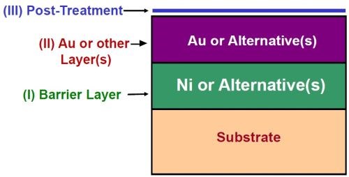
Figure 1 - Schematic diagram of nickel-gold system.
However, increasing demands on reliability have resulted in the implementation of more stringent requirements, particularly with regard to corrosion protection. For example, as integrated circuit (IC) semiconductor devices and printed circuit board (PCB) dimensions have been scaled down, the geometric demands on the electronic interconnects have increased dramatically. Hence, the development of more robust alternatives to the nickel/gold system have become essential.
This paper deals with a number of those alternative technologies, first in terms of improved barrier layers, then alternatives to gold and the post-treatment processes, and finally emerging applications requiring completely new electronic finishes.
Improved Barrier Layers
The traditional barrier layer for electronics finishes is matte nickel sulfamate. It has served the industry well over the years, but miniaturization and increased geometric complexities have presented challenges which exceed the limits of the coating. Corrosion resistance at lower deposit thicknesses, increased thickness distribution in low current density areas and low internal stress requirements are harder to meet with the traditional process. Alternate processes are available which have shown success in meeting the new specifications, including nanocrystalline nickel and nickel-free cobalt-tungsten processes.
Nanocrystalline nickel
Nano-crystalline nickel is an advanced nickel electroplating process specifically engineered to significantly improve nickel thickness distribution and corrosion-resistance from a proprietary electrolyte in high speed/reel-to-reel plating applications. The process yields a semi-bright, low stress, ductile deposit. The grain size is on a nanoscale, approaching an amorphous deposit. Comparative properties are shown in Table 1 for the nanocrystalline and sulfamate nickel deposits. The lower stress and increased hardness exhibited by the nanocrystalline nickel maintain a protective barrier layer in smaller geometries.
Table 1 - Comparative properties of nanocrystalline and sulfamate nickel.
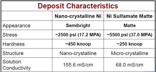
The higher solution conductivity suggests improved throwing power. This is borne out by the data for the connector design shown in Fig. 2, where the thickness distribution is improved by 30 to 40% with the use of nanocrystalline nickel (data in red).
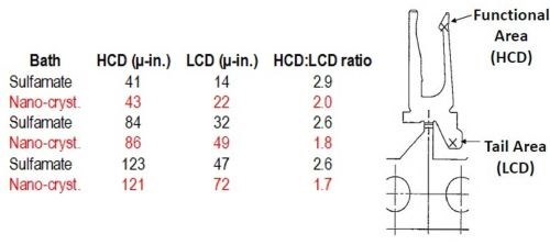
Figure 2 - Comparison of throwing power of nanocrystalline and sulfamate nickel.
Corrosion resistance for the nanocrystalline nickel is also superior to the standard sulfamate deposit, as shown in Fig. 3 after a two-hour nitric acid vapor exposure test.
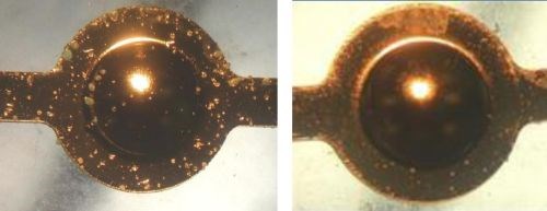
Figure 3 - 2-hr nitric acid vapor test results: (L) Sulfamate Ni - 120 μ-in., Au - 30 μ-in.; (R) Nano Ni - 100 μ-in., Au - 30 μ-in.
Cobalt-tungsten
For certain applications, the elimination of nickel entirely from the plated layer system is desirable (for example, the issue of nickel dermatitis). Cobalt-tungsten alloy (CoW) barrier layer electroplating technology has been developed for these applications. The alloy deposit composition is 65/35 Co/W (±5%). Its structure is also nanocrystalline (Fig. 4), exhibiting a hardness of 600-700 VHN. Deposit stress is low and corrosion resistance is excellent.
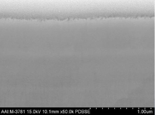
Figure 4 - FIB/SEM cross-section of CoW (50,000X)
In production, the process offers a wide operating window and serves as a drop-in replacement for nickel or nickel-tungsten plating solutions in existing process lines. It is suitable for consumer applications, in that it is a nickel-free deposit that poses no nickel dermatitis issues.
Alternatives to Gold/Posttreatment Processes
The search for alternatives to gold plating is often motivated by matters of cost. One of the more promising alternatives is the use of silver with an appropriate posttreatment. Until today, two technical issues have limited silver’s implementation in non-automotive applications:
- Wear resistance especially after multiple insertion cycles and
- Corrosion resistance (for example, overcoming the silver tarnish issue).
The automotive use of silver is currently restricted to sealed applications with minimal insertions. An ideal solution would be a wear-resistant / corrosion resistant silver plating process. Conventional silver, however, exhibits a high friction coefficient of about 1.2, as plated and after baking. One promising option is the use of silver alloy plating.
Silver alloy plating
Silver alloy plating can now be produced from a proprietary two-part system consisting of a silver alloy electroplated deposit and a unique post-treatment process chemistry***. This combination provides excellent deposit conductivity combined with superior corrosion properties and significantly improved wear resistance when compared to conventional silver.
The deposit hardness is 175 KHN as plated, decreasing to 145 KHN after a baking process. The contact resistance is low and stable, at ~2.5 m-Ω after bake, as well as after 20 days of exposure of mixed flow gas (MFG) testing. Wear resistance is also stable, with a coefficient of friction of ~0.2 under the same bake and over the 20-day MFG test conditions. Corrosion resistance testing shows minimal to no corrosion after 20 days exposure to MFG testing. Solderability testing passes J-STD-002C after a 500-hr bake.
The silver alloy process is supplemented with an inorganic nano-coating. This system passed sulfur corrosion testing, consisting of a full immersion of parts in a 5% potassium sulfide (K2S) solution for 5 minutes (Fig. 5). Similar results were observed with five-days of MFG exposure per EIA-364-65B, Class IIa.
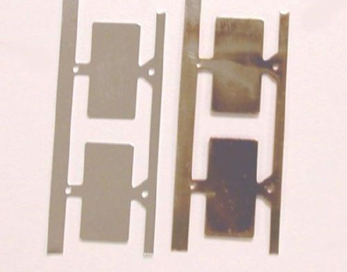
Figure 5 - Sulfur corrosion test results for a silver alloy coating (L) with and (R) without an inorganic nano-coat post treatment.
For silver then, several options exist, including silver alloy plating + post-treatment, silver plating with a nano-coating for corrosion protection only, and silver plating with a two-step post-treatment process sequence consisting of a nano-coating + post-dip (lube). Improvements in both silver protection and wear resistance can be achieved. These combinations provide similar technical performance comparable to hard gold in connector and related applications.
Emerging Applications Requiring New Electronic Finishes
The electronics finishing field continues to be presented with new challenges as new applications emerge. Significant among these are electrolytic sweat-resistant connector finishes required in the mobile phone arena, press-fit connector pins and high-frequency (5G) applications.
Electrolytic Sweat-resistant (ESR) Connector Finishes
Two recent changes in cell phone technology are having a major impact on the plated finishes used for mobile phone connectors. The first is the replacement of the traditional headphone jack with a single connector that performs both the electrical charging function and the headphone connection. The second is the implementation of “quick-charge” connector technology. When mobile phones first became common, conventional charging involved a 5 V / 1 A, or 1.0 W charge regimen. Through three generations of “quick-charge” development, dynamic charging, involving up to 18 W are common today.
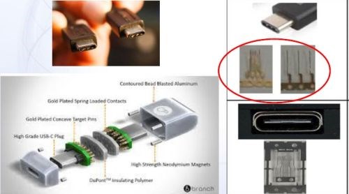
Figure 6 - Configuration and construction of USB-C connector pins.
Both of these factors have affected mobile phone connector technology. Consumers who exercise while using head phones and/or charging their cell phones and thus handling the connector itself, results in human sweat being present on the plated connector in the presence of electrical current. Human sweat serves as an electrolyte, and thus corrosion can occur. This electrolytic sweat-induced corrosion issue is made more severe when combined with the higher charging current/volts of quick charge technology. The complexity and variety of materials in a connector pin (Fig. 6) adds to the challenge.
Another challenge is the need for a realistic corrosion test to replicate the conditions involving human sweat induced corrosion. Conventional exposure tests involve specimen placement in a corrosive atmosphere, such as nitric acid fumes in NAV testing or sodium chloride salt mist in neutral salt spray (NSS) testing. The corrosion occurs from the outside of the connector to the inside. With human sweat exposure, the connector is virtually immersed in the electrolyte, and corrosion occurs from the inside to the outside.
Hence, an electrolytic sweat resistance (ESR) test is used, with an anodic charge applied to the connector immersed in an artificial sweat electrolyte (basically a modified NaCl solution) (Fig. 7).
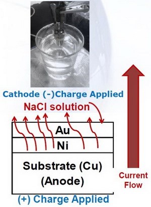
Figure 7 - Electrolytic sweat test.
Extensive testing in our laboratory indicates a number of points in processing that are essential for the system to meet these test specifications. The preparation of the basis copper surface is critical, and an extremely corrosion-resistant barrier layer (or layers) is required. For high end applications, nickel cannot be used.
A top layer of gold cannot be used, as it is easily attack during the ESR testing. Instead, a rhodium-containing (Rh) deposit is necessary, as it is resistant to the artificial sweat solution.
Ultimately, the optimal layer system to be selected depends on a trade-off of performance vs. cost.
Press-fit connector pins
The introduction of connector press-fit pin applications (Fig. 8) has led to new developments. The use of matte tin plate in these applications has resulted in extremely long whiskers under certain press-fit conditions. Whiskers can create short-circuits. Fast growth of whiskers is observed in press-fit connections because of high mechanical stress at the pure tin surfaces. In some cases, whisker lengths greater than 2 mm have been observed within two to six weeks after insertion.
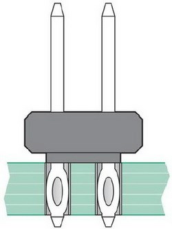
Figure 8 - Connector press-fit pin configuration.
Connector companies and/or end users have been experimenting with various non-tin solutions for years. Recently two alternative finishes have emerged as potential solutions for press-fit pin whiskers formed under compression. Tin alloys (Sn-Ag, Sn-Bi, Sn-Pb) over nickel have shown promise, but a tin-free layer of indium has shown significant performance improvement (Fig. 9).† Indeed, indium is now a qualified/specified finish for some press-fit applications. Beyond this, bismuth is also being considered as an option for certain applications.
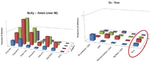
Figure 9 - Tin whisker performance test results for a variety of coatings: (L) tin alloys over nickel and (R) tin-free systems.† Some of the systems, while showing good performance, have other drawbacks, e.g., toxicity considerations for Sn-Pb.
Connector finishes for high-frequency applications (5G)
5G communications and attendant high-frequencies are rapidly coming online. Again, this new regimen poses challenges in electronic finishes. In this case, it has been found that design of the PCB final finish must take high-frequency signal loss into account. As shown in Fig. 10, additional high-frequency signal loss is encountered with the presence of the standard electroless nickel / immersion gold (ENIG) system. It has been found that the nickel deposit is the primary source of this signal loss.††
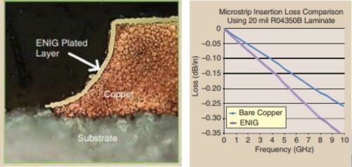
Figure 10- High-frequency signal loss for bare copper vs. ENIG connector finish.
Studies have shown that the connector finish necessary to minimize signal loss requires a nickel-free barrier layer, plus good conductivity and corrosion resistance for the final finish. Palladium (Pd) is a suitable deposit that can function as both a barrier layer and a final finish. However, barrier layer effectiveness requires relatively a high thickness (>0.75-1.0 μm), and electroplated palladium is notorious for micro-cracking at high thicknesses.
The solution is a proprietary micro-crack free palladium process (Fig. 11). This process produces low stress deposits, with no spontaneous microcracking observed up to a palladium thickness of 4 μm. Thicknesses of up to 2 μm have been shown to resist cracking during bending. The process operates at a neutral pH and exhibits no ammonia smell. It is a table electrolyte with a wide current density range.
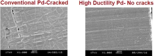
Figure 11 - Comparison of conventional palladium vs. low stress, high ductility crack free palladium for 5G applications requiring reduced high-frequency signal loss.
Conclusions
- Rapid changes are occurring in an industry where conventional Ni/Au has been used for four decades.
- Alternative finishes are being considered and/or implemented, including exotic materials never before considered feasible in a connector application (Fig. 12).
- We expect additional changes will occur as connector finish technology needs to keep up with the demands of the other interconnects and/or use environments.
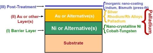
Figure 12- Summary of new systems available to meet the demands of future electronic finishing technology.
About the author

Rob Schetty is a Vice President for Technic, where he has responsibility for worldwide plating chemical technology for electronic components, lead frames and connectors. Rob received his Bachelor of Science degree in Chemical Engineering from the University of Pennsylvania in Philadelphia, PA, USA. Rob has been with Technic for 18 years and has been in the plating industry for over thirty years, including senior positions in R&D, marketing, business development and a multi-year assignment in Asia. Rob has expertise in many aspects of electroplating and holds multiple US and foreign patents, and is considered one of the global experts in electronics plating. In addition, Rob has published over twenty papers and a textbook chapter related to electronic and industrial metals plating and has presented at a multitude of international industry conferences and seminars.
*Compiled by Dr. James H. Lindsay, Technical Editor - NASF
**Corresponding author:
Rob Schetty
Technic Advanced Technology Division
Technic Inc.
111 E. Ames Court
Plainview, NY 11803
Phone: (516) 349-0700; X19
Mobile: (516) 375-1296
E-mail: rschetty@technic.com
*** Durasil™, Technic Inc., 111 E. Ames Court, Plainview, NY 11803
†Source: Dr. Hans-Peter Tranitz, “Whiskers and Alternative Surface Finishes in Press-in Technology”, Continental Automotive GmbH, D-93055 Regensburg, Germany.
†† Source: John Conrood, “Ambiguous Influences Affecting Insertion Loss of Microwave Printed Circuit Boards, IEEE Microwave, Issue 1527-3342/12
Related Content
Successful South African Plater Beating the Odds
Remaining focused on quality and reliability, Team Plating Works stays profitable in a volatile and challenging economy.
Read More3 Tests to Ensure Parts are Clean Prior to Plating
Making sure that all of the pre-processing fluids are removed prior to plating is not as simple as it seems. Rich Held of Haviland Products outlines three tests that can help verify that your parts are clean.
Read MoreProducts Finishing Reveals 2023 Qualifying Top Shops
Each year PF conducts its Top Shops Benchmarking Survey, offering shops a tool to better understand their overall performance in the industry. The program also recognizes shops that meet a set of criteria to qualify as Top Shops.
Read MoreAn Overview of Electroless Nickel Plating
By definition, electroless plating is metal deposition by a controlled chemical reaction.
Read MoreRead Next
A ‘Clean’ Agenda Offers Unique Presentations in Chicago
The 2024 Parts Cleaning Conference, co-located with the International Manufacturing Technology Show, includes presentations by several speakers who are new to the conference and topics that have not been covered in past editions of this event.
Read MoreEpisode 45: An Interview with Chandler Mancuso, MacDermid Envio Solutions
Chandler Mancuso, technical director with MacDermid Envio discusses updating your wastewater treatment system and implementing materials recycling solutions to increase efficiencies, control costs and reduce environmental impact.
Read MoreDelivering Increased Benefits to Greenhouse Films
Baystar's Borstar technology is helping customers deliver better, more reliable production methods to greenhouse agriculture.
Read More


