Bright Future for Plating LED Lights
LEDs are widely used in the electronics and automotive industries, together with household and road lighting applications. Silver plating of the LED substrate can be carried out via conventional rack or reel-to-reel plating procedures.
Most industrial nations have gradually removed incandescent light bulbs from the market due to their inadequate performance and high consumption of electricity.
In 2008, the European Union began the process, and in 2012, the last incandescent bulb was sold and the rest removed from the shelves the following day—marking the end of a technology era that had caused a revolution when it was introduced about 130 years ago.
The U.S. Congress passed a law in 2007 to begin phasing out the old familiar tungsten-filament 40- and 60-watt incandescent light bulbs by the beginning of 2014.
Light emitting diode (LED) technology provides an efficient alternative to standard bulb technologies. The efficiency of each lamp type can be expressed as “luminous efficacy,” defined as the ratio of the luminous flux emitted from the lamp per electrical power required by the lamp.
Efficacy is specified in lumen [lm] per watt [W-1] and is typically 15 lm/W for conventional light bulbs, increasing to 30 lm/W for halogen, while as high as 150 lm/W for an LED. This high efficiency, combined with extended longevity, explains why LED technology has high market attraction with excellent growth and application potential.
A low free-cyanide silver process, containing innovative brightener additives, enables the highest luminous reflectance and performance of the LED.
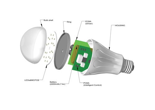
The inner workings of a typical LED light.
Photo courtesy of Smartcharge.
Highly Reflective Coatings
Nowadays, LEDs are widely used in the electronics and automotive industries, together with household and road lighting applications. Silver plating of the LED substrate can be carried out via conventional rack or reel-to-reel plating procedures. The current density range used can vary considerably, typically 20 to 150 A/dm2, dependent on whether the surface is fully or partially (spot) plated.
Insoluble anodes are used in these high-speed silver processes with the inevitable release of small amounts of free cyanide during electrodeposition. The silver coating must possess excellent reflectivity to meet the requirements needed for the manufacture of the high-power LEDs used in TV screens.
Reflectivity can normally be measured using either a transmission densitometer, providing a GAM value, or by measuring the angular distribution of diffused light of a defined wavelength emitted from an irradiated sample. The densitometer quantitatively determines the color density, or the amount of color per unit of area.
During measurement, a defined wavelength light source is irradiated onto the respective coating and the reflected light photo-electrically measured (remission value). The measured density values (often called GAM readings) typically lie between 0.0001 and 2.0. The name is derived from the original densitometer manufacturer, G.A.M Co., and is now widely accepted as the industry standard.
The larger the GAM value, the higher the reflectivity of the surface. For LED applications, different GAM values are required for the respective LED performance with 1.2–1.4 for the lower range and 1.8–2.0 for the upper range.
Future LED generations require GAM values greater than 2.0, and in order to meet these requirements, novel silver plating brightener systems have been developed for both rack and reel-to-reel applications. The new Silvertech LS LED and Silvertech HS LED processes contain zero or minimal levels of free cyanide, thereby enabling the use of inert anodes. Typical deposit hardness values of 120–140 Hv can be achieved, and for reel-to-reel spot plating applications, current densities as high as 150 A/dm2 may be used.
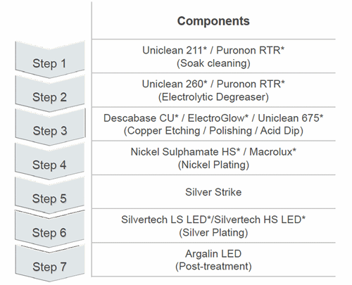
Samples were prepared using this process sequence with pretreatment and layer combination variance.
A degree of variance also occurs with the deposited layer structure prior to the final bright, highly-reflective silver coating. For example, the LED substrate (circuit boards, ceramics) are initially copper plated, followed by a nickel barrier layer prior to silver plating. For the plating of leadframes, it is also possible to directly apply the silver onto a highly levelled copper electrodeposit as an alternative to the nickel barrier layer. Alternatively, overall brightness improvement can be accomplished by pretreatment modifications such as the introduction of electropolishing or micro-etching steps.
Extensive studies have been carried out investigating the effect of process sequence, including pretreatment and type of nickel process used (matt or bright) on the final coating brightness and reflectivity properties.
Surface reflectivity was determined using both a densitometer and a diffused light measurement.
The second method, based on diffused light measurement, comprises a surface irradiated by a light beam of diameter “d.” If the surface is perfectly smooth (perfect mirror), the reflected light is identical to the incident beam. However, if the surface is not perfect, rough diffused light appears together with the reflected light. This diffused light provides the angular distribution of the beam, with values increasing with increase in surface roughness.
Silver Layer
Samples were prepared using the following process sequence with pretreatment and layer combination variance. The leadframe substrate used throughout was C194 copper alloy.
In an initial test series, silver spot plating at 50,100 and 150 A/dm2 was carried out directly onto the copper alloy substrate. The high-speed silver electrolyte contained 70 g/l Ag at pH 8.5. The deposit thickness was 5 µm and the solution temperature was fixed at 65°C and 45°C.
Average GAM values of 2.0 were observed for all selected current density/ temperature combinations. A second test series was then carried out with pretreatment and nickel (bright or matt) variation.
Reflectivity measurement was carried out on the substrate before and after surface activation with the various pretreatments (leg 1–4), on nickel layers (leg 5–10) and also after silver strike (leg 11–16). Furthermore, a correlation between the GAM value, the diffused light value and the relative surface area increase (RSAI) was also established.
RSAI roughness values are normally measured using an interference microscope and calculated from a topographic comparison of the sample’s three-dimensional surface mapping and its two-dimensional projection. An RSAI value of 100 percent would mean a doubling of the surface area.

The graph above presents the three different measurement values for all 16 test combinations. It clearly shows the enhanced diffused light readings and the excellent correlation between all three techniques. High Optosurf values correlate with an increased surface roughness (RSAI) and hence low light reflectivity (GAM). An RSAI value of 5.39 (leg 3) corresponds to a 5.39 percent increase in surface area, whilst the best surface condition (mirror bright) of 0.04 is as expected from a polished surface with a highly levelled nickel interlayer (leg 15).
In general, the use of a bright nickel barrier layer provides significantly lower diffused light values and higher GAM readings, whereas a silver strike layer causes a negative effect. Electropolishing further improves values of the base material.
The leg 14 conditions were then used for further high-speed silver plating tests (100 A/dm2, 60 g Ag/L) at varying brightener concentration (1–10 mL) for a 5µm deposit. In all cases, GAM values of over 2.0 were achieved with best results at a brightener concentration of 2–3 mL/L.
A further test series was carried out at 50 A/dm2 for varying g/L silver in the electrolyte. Results show an expected reduction in GAM value at increasing silver concentration. This optimized silver process containing the new brightener system was tested at a selected customer.
Initial tests were carried out using an electrolyte containing 60 g/L Ag over a current density range of 70 to 100 A/dm2 for a standard brightener system and using alloy C194 as substrate. Deposits showed poor brightness uniformity and GAM readings could not be measured.
A repeat series of tests was then carried out using the new silver brightener system, achieving consistent GAM values of 2.0 and above. In addition, silver was deposited onto both bright and matt nickel interlayers, providing greater than 2.0 GAM readings in each case.
Separate measurements were carried out on both selective silver (spot) and the nickel interlayer (background), providing a 0.4 GAM value for matt nickel compared with 2.34 for bright nickel.
The high GAM results (regardless of the nickel interlayer) highlights the advantage of the new silver brightener system in providing the high levelling characteristic needed to achieve the required reflectivity without using nickel levelling additives. Hence the technical functionality (bondability) of the silver may be maintained even after heat treatment, compared with the expected negative effect (due to the higher organic content) when a bright nickel barrier layer is used.
Effect of Heat Treatment
The same customer site was used to evaluate the effect of heat treatment for the new brightener system. Silver deposits were heated for one hour at 200°C and for two hours at 170°C. As expected, subsequent GAM measurements showed significant reflectivity losses.
A new post-dip was developed to prevent reflectivity loss due to heat treatment of silver coatings. Tests were carried out to highlight the benefit of this aqueous post-treatment, which uses organic additives to effectively prevent discoloration due to heat exposure.
All test samples were heated to 200°C for an extended duration of two hours, with GAM measurements at varying post-dip immersion times. A similar loss in GAM reading could only be observed for the shortest immersion time of three seconds. Consistent GAM readings were maintained for higher immersion periods with no observed discoloration of the silver deposit.
To confirm the effectiveness of the post-dip, irrespective of nickel type, a final test series was carried out for both bright and matt nickel interlayer. Immersion times ranged from 10 to 60 seconds and the test samples were heated to 310°C for 15 minutes after the final post-dip treatment.
Within experimental accuracy, these GAM results clearly confirm the effectiveness of the post dip treatment, irrespective of the interlayer nickel type used.
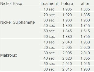
GAM measurements before and after heat treatment.
Summary
Functional silver coatings that provide ultimate reflectivity are required for future generations of high-power, energy-saving LEDs. This reflectivity property is normally measured using a light transmission densitometer and expressed as a GAM reading. For the type of LED described in this paper, GAM values of greater than or equal to 2.0 are required.
To meet these requirements, a new low free-cyanide silver brightener system has been developed, providing mirror-bright deposits over a wide current density range (to 150 A/dm2). Investigative work included the effect of substrate pretreatment. Acid activation, micro-etching and electropolishing were all assessed, with the latter providing expected benefits, confirmed by GAM and diffused light readings. Optical properties were further enhanced when the interlayer nickel type was replaced with a high levelling brightener system. As expected, the brightener-free silver strike step provided a loss of brightness.
These studies also highlighted the exceptional levelling properties of the new silver brightener system in achieving the target of greater than or equal to 2 GAM value, irrespective of which nickel interlayer type was used. A new post dip treatment was also developed and its effectiveness demonstrated, providing minimum silver discoloration after heat treatment for both 200°C at two hours and 310°C at 15-minute conditions.
Originally published in the September 2015 issue.
Related Content
Checon Expands Market Offering with Acquisition of Umicore Electrical Materials USA, Inc.
The company is strategically working to meet future growth opportunities surrounding the use of precious metals and conductive materials like copper and aluminum.
Read MoreFinishing High Reliability, Function Critical Parts
From safety critical automotive and aerospace components to lifesaving medical micro-components and implantable devices, Indiana-based Electro-Spec finishes applications that require zero failure rates.
Read MoreRead Next
Education Bringing Cleaning to Machining
Debuting new speakers and cleaning technology content during this half-day workshop co-located with IMTS 2024.
Read MoreEpisode 45: An Interview with Chandler Mancuso, MacDermid Envio Solutions
Chandler Mancuso, technical director with MacDermid Envio discusses updating your wastewater treatment system and implementing materials recycling solutions to increase efficiencies, control costs and reduce environmental impact.
Read MoreDelivering Increased Benefits to Greenhouse Films
Baystar's Borstar technology is helping customers deliver better, more reliable production methods to greenhouse agriculture.
Read More









.jpg;maxWidth=300;quality=90)


