Chromium-free Etching and Palladium-free Plating of Plastics
Plastics are replacing metals in the manufacture of many parts, and quite often there is a need for metallic coatings on the plastics and other non-conductors. This paper will describe new processes of preparing ABS plastic substrates for subsequent metallization.
A printable PDF version of this paper is available by clicking HERE.
By Vijaykumar Ijeri, Komal Shah and Snehal Bane, Grauer & Weil (India) Ltd., Mumbai, India
ABSTRACT
As plastics are replacing many of the metal parts, there is often a need to have metallic coatings on plastics and other non-conductors. This paper will describe new processes of preparing ABS plastic substrates for subsequent metallization. A process replacing the traditional chromic acid etching step with a room temperature, environmentally-friendly etchant is described. The etchant gives the plastic substrate an increased hydrophilic surface and a microroughened, microporous resin topography.
Further, due to the high cost of palladium there is a need for a palladium-free activator. A non-precious metal activator useful for obtaining uniform, adherent coatings of metal layers on plastic substrates has been developed. The resultant colloidal solution is active and believed to adsorb on the hydrophilic surfaces of the etched plastic. A specific reducing agent is used to transform the adsorbed complex into a conductive layer which allows the plating of subsequent conducting metal layers. The possibilities of direct electroplating (without an electroless step) are also discussed.
Keywords: Plating on plastics, chromium-free etchant, palladium-free activation, hexavalent chromium substitutes
Introduction
Rapid advances in polymer chemistry and production technology have resulted in the replacement of metals by plastics in a wide range of applications. Plastics provide the advantages of weight reduction, ease of fabrication and design flexibility. The electroplating of plastics was introduced commercially in Europe and North America in the early 1960s with limited acceptance. The major breakthrough that led to growth in the industry was the development of chemical processes for the surface preparation of acrylonitrile-butadiene-styrene (ABS), which enabled good bonding to be obtained between the plastic substrate and the metallic coating. The major driving force for plating-on-plastics (POP) was the automotive industry. The need for increased fuel efficiency called for a reduction in vehicle weight. Consequently, plastics were found to be useful in automotive components. Bright finishes have a popular aesthetic appeal, which is achieved by nickel/chromium plating. ABS remains the most widely used plastic for plating applications and excellent quality is obtained routinely in the industry. Metal-plated plastics find use in the automotive industry, hardware, plumbing fixtures, knobs, RFI/EMI-shielding and electronic applications.
Prior to electroplating, the plastic surface needs to be treated and made conductive. This generally involves the following steps:
- Cleaning in mild alkaline solution with surfactants, which removes any dirt accumulated on the parts during handling.
- Etching of the plastic to provide hydrophilic and micro-roughened surface that is useful for adhesion of subsequent layers of coatings.
- Activation of the etched surface to produce catalytic sites that will enable chemical deposition of nickel or copper to form a thin conductive top layer.
Once this conductive layer is formed, the parts can be electroplated with copper, nickel and chromium. This paper will discuss the developments in etching and activation processes leading to an overall economical and environmentally-friendly plating system.
Etching
ABS is a thermoplastic terpolymer that has an acrylonitrile-styrene matrix with butadiene rubber uniformly distributed in it. This quality makes it unique for plating, as the butadiene can be selectively etched out of the matrix (Fig. 1), leaving microscopic holes that are used as bonding sites for activation and electroless deposits. Other factors influencing the choice are low cost, low thermal expansion, ease of molding, good metal adhesion to the substrate and good appearance after plating.

Figure 1 - Schematic diagram of butadiene rubber in ABS plastic (L) and the etched ABS plastic surface (R).
The etching solutions normally used are made from mixtures of chromic acid and sulfuric acid. Typically they contain 375-425 g/L CrO3 and 180-220 mL/L H2SO4 and are operated at 50-65°C.
The toxicity of chromic acid, more specifically in the plating industry, was recognized several decades ago.1,2 The Restriction of Hazardous Substances Directive (RoHS) issued in 2007, asked to ban several toxic substances including hexavalent chromium. Hexavalent chromium plating has been classified by the U.S. Environmental Protection Agency (EPA) as an environmentally-unfriendly process. These policies have stimulated search for a cleaner alternatives to hexavalent chromium.
The etching or dissolving of the butadiene phase in ABS requires strong oxidizing agents and an acidic medium. A recently developed proprietary chromium-free etchant for ABS plastics, accomplishes two purposes: (1) making the surface hydrophilic and forming microscopic holes in the surface of the plastic to provide the bonding sites for activation and metal deposition. These sites are needed for adhesion between the plastic and the metal.
The main difference between metallic and nonmetallic surfaces is the nature of the bond between substrate and coating. While adhesion to metal is of an atomic nature, the adhesion to organic and inorganic substrates is primarily mechanical. The basis for obtaining adhesion to these materials is to develop the proper surface morphology by means of chemical or mechanical treatment. The chromium-free etchant gives the desired morphology to anchor the colloidal Sn-Pd activator (Fig. 2).
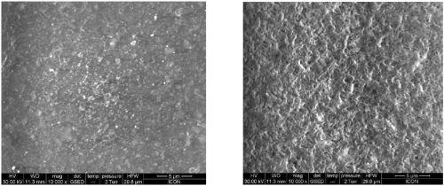
Figure 2 - Scanning electron micrographs of (L) non-etched ABS plastic and (R) ABS plastic etched in the proprietary chromium-free process.
The chromium-free etchant is very convenient as it is operated at room temperature (20-30°C) and it emits no fumes. The process sequence is the same as that used with chromic-sulfuric etchants, and hence can be easily adapted in a plating shop (Fig. 3). A chromium neutralization step is not required in this process.
An adhesion test is important for determining etchant performance. Poor adhesion, indicated by the peeling away of the electroplated layers (i.e., separation at the metal-plastic interface) is an indication of ineffective etching. The adhesion achieved by the chromium-free etchant was verified by a 90° bend test. Further, mechanical adhesion between the metal layer and the ABS substrate was studied by a qualitative Scotch tape test as described in ASTM D3359. This method consists of applying and quickly removing pressure-sensitive adhesive tape over sixteen 1 × 1-mm cross-hatched squares. This standard test allows a direct comparison of the adhesion of films obtained under various conditions on similar substrates. In all cases (etched either in chromic acid or in the Cr-free process) only 0-5% area was peeled away.
Thermal cycling of plated parts according to ASTM B604-91 showed no blistering, peeling or distortions of the coatings.
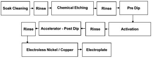
Figure 3 - Typical process sequence for plating on ABS plastics.
Figure 4 shows samples of plated plastic parts that have been processed using the proprietary chromium-free etch solution. It can be seen that the surface appearance is very good. When compared with finishes produced with chromic-sulfuric acid etches, there is no discernible difference in appearance.

Figure 4 - The image on the left shows plated ABS ring pieces using the process sequence shown in Fig. 3: (L) after electroless Ni; (C) after electroless Ni + acid copper and (R) electroless Ni + acid Cu + bright Ni. The image on the right is of a Cu-Ni-Cr deposit on ABS components.
Activator/Catalyst
Nonmetallic surfaces lack catalytic properties and therefore require activating treatments that will render them catalytic. In general, this activation is done by seeding the surface with a catalytically active metal, usually from palladium and tin salts. The parts are then plated with electroless nickel or copper. This forms the conductive base for the electroplating steps to follow.
The catalyst or activator bath contains a colloidal suspension of palladium and tin ions. The function of this bath is to deposit the colloidal palladium into the surface cavities of the part to be plated. Palladium is a catalytic metal that causes the subsequent reduction of copper or nickel to form a continuous conductive layer. This deposition is aided by the dissimilar charges of the plastic and catalyst. The plastic becomes positively charged during the oxidation of the surface molecules.3
After activation, the parts pass through an acceleration step. The accelerator is typically composed of organic / mineral acid solution or mixtures thereof. The function of this bath is to remove the excess tin ions from around the palladium nuclei that were deposited in the activator bath to promote quicker reaction initiation in the following electroless deposition step.
CuSO4 + 2HCHO + 4NaOH → Cu + Na2SO4 + 2NaCOOH + 2H2O + H2
NiSO4 + 3NaPO2H2+ 3H2O → Ni + 3NaH2PO3 + H2SO4 + 2H2
The metal ions receive electrons from the reducing agents (formaldehyde, sodium hypophosphite, etc.) changing them from ionic to a metallic form. The rate of deposition and thickness of the deposit are governed by temperature, time and concentration.
The Pd-Sn activator bath is a very expensive chemical bath, and thus there is a need for a palladium-free activator in the market. A proprietary activator comprising multiple metals from among the transition metals or d-block elements. An appropriate combination of metal salts and complexes provide for the catalytic activity on the surface for the subsequent metallization process. The different possibilities, including direct plating, are shown in Fig. 5.
A conventional way would be to deposit copper from an electroless bath after activation and post activation steps. Thereafter, layers of nickel and chromium are electroplated onto it (Fig. 6 and 7). Another route is to electroplate directly with nickel after the post-activation stage.
The palladium-free activator is also a colloidal solution. The size of colloids has a profound impact on coverage and skipping. The activator must be present on every area to be plated. If for any reason, the catalyst is not present on the surface of the part, a plating void, or “skip plate,” will occur. This skip plate defect can result from poor catalyst absorption or catalyst removal from the surface. Hence, the smaller the colloidal size the better will be the coverage and the lesser the consumption.
Ultrasonic vibrations were used to reduce the particle size of the colloids. The best results in terms of coverage and consumption were obtained when the particle size dispersion was less than 1,000 nm (Fig. 8).
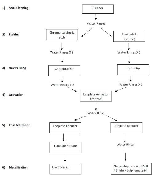
Figure 5 - Chromium-free, palladium-free and direct plating possibilities.
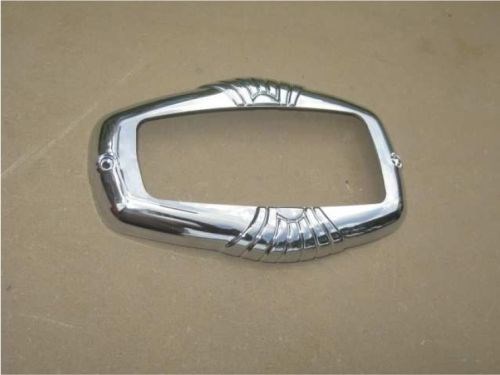
Figure 6 - An ABS component electroplated with Cu+Ni+Cr after palladium-free activation and electroless copper.
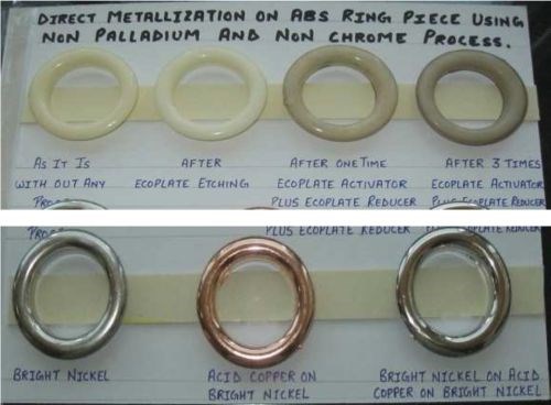
Figure 7 - Appearance of ABS pieces after each step in the ECOPLATE palladium-free activation process.
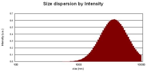
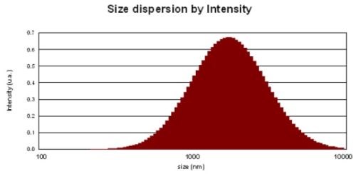
Figure 8 - Particle size distribution of Pd-free colloidal activator: (top) as-prepared and (bottom) after ultrasonication for 20 min.
The term “direct plating” or “direct metallization” in the technology of plating on plastics means the process of electroplating of the plastic material without going through the electroless Cu/Ni step. This has the advantage of reduced number of steps in the overall process.
After the palladium-free activation, it is possible to proceed to either electroless copper deposition or nickel electroplating. The intermediate step involves a reducer that converts the activator film into a catalytic conductive / semi-conductive layer which enables electroless deposition of copper from regular formaldehyde baths or direct electrodeposition of nickel from sulfate or sulfamate baths.
Images of cross-sections of ABS plated by the direct metallization process are shown in Fig. 9. Adhesion between layers is maintained even at high thicknesses.
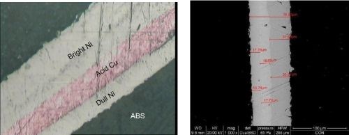
Figure 9 - Cross section of multilayered plating by the direct metallization process: (L) optical microscope image and (R) SEM image.
Conclusions
New options for plating on plastics have been presented in this paper. The use of chromium-free etchant provides several advantages, such as:
- Freedom from carcinogenic hexavalent chromium,
- Freedom from ozone-depleting and bioaccumulative fluorocarbon chemicals that are used to prevent chromium mist,
- Fume-free operation at room temperature, which is worker friendly.
Further, in combination with palladium-free and direct plating options, it is possible to plate on ABS with an environmentally-friendly and cost effective process.
Note: Coating thickness and imaging of surface morphology was done by scanning electron microscopy (FEI–Quanta 200 ESEM, Netherlands).
References
1. H. Royle, Environmental Research, 10 (1), 141-163 (1975).
2. S. Katz & H. Salem, J. Appl. Toxicology, 13 (3), 217-224 (1993).
3. R.L. Cohen & K.W. West, J. Electrochem. Soc., 120 (4), 502-508 (1973).
Related Content
Finishing Systems Provider Celebrates 150 Years, Looks to Future
From humble beginnings as an Indiana-based tin shop, Koch Finishing Systems has evolved into one of the most trusted finishing equipment providers in the industry.
Read MoreTop Shop Aces Outstanding Customer Service
More than a finishing shop, this anodizing, powder coating and vacuum resin impregnating business goes above and beyond for its customers by being a resource for whatever their finishing needs might demand.
Read MoreUnderstanding and Managing White Spots on Anodized Aluminum
Having trouble with spotting defects when anodizing? Taj Patel of Techevon LLC offers a helpful overview of the various causes of white spots and potential solutions.
Read MoreProducts Finishing Reveals 2024 Qualifying Top Shops
PF reveals the qualifying shops in its annual Top Shops Benchmarking Survey — a program designed to offer shops insights into their overall performance in the industry.
Read MoreRead Next
Delivering Increased Benefits to Greenhouse Films
Baystar's Borstar technology is helping customers deliver better, more reliable production methods to greenhouse agriculture.
Read MoreA ‘Clean’ Agenda Offers Unique Presentations in Chicago
The 2024 Parts Cleaning Conference, co-located with the International Manufacturing Technology Show, includes presentations by several speakers who are new to the conference and topics that have not been covered in past editions of this event.
Read MoreEducation Bringing Cleaning to Machining
Debuting new speakers and cleaning technology content during this half-day workshop co-located with IMTS 2024.
Read More




.jpg;maxWidth=300;quality=90)


