Electroplating, Electrochemistry and Electronics - The 15th William Blum Lecture - Part 2
This article is the second of four parts of a re-publication of the 15th William Blum Lecture, presented at the 61st AES Annual Convention in Chicago, Illinois, on June 17, 1974. Dr. George Dubpernell reviews the history and extent of commercial plating, then delves into the electrochemical science, including potentials, overvoltage and connections to electronics.
by
George Dubpernell
M&T Chemicals
Ferndale, Michigan
Recipient of the 1973 William Blum
AES Scientific Achievement Award
Editor’s Note: Originally published as Plating & Surface Finishing, 62 (5), 436-442 (1975), this article is the second of four parts of a re-publication of the 15th William Blum Lecture, presented at the 61st AES Annual Convention in Chicago, Illinois, on June 17, 1974. A printable PDF version of Part 2 is available by clicking HERE. The printable PDF version of the complete 44-page paper is available HERE.
Experimental
The writer first attempted61 to separate overvoltage into measurable component parts by the use of extremely thin platinum and palladium membranes, with hydrogen or oxygen being evolved on one side of the membrane only, and the potential of the other side checked for diffusion products of an electromotively active nature. No diffusion of electromotively active hydrogen or oxygen was detected. Instead, there appeared to be no diffusion whatsoever with the thicker membranes. When the membrane was made thin enough, some current penetrated solution in fine pores and charged the back side of the membrane.
In the discussion to Coehn's paper in 1899,57 Ostwald suggested that possibly overvoltage was due to the formation of atomic hydrogen at the cathode, and Bredig described his work with Haber on the alloying of sodium with lead, tin and mercury, as a possible clue to the nature of overvoltage phenomena.
Since no electromotively active hydrogen was detected in the first experiments,61 the writer became imbued with the idea that the high negative potentials of cathodic overvoltage were due to the electrodeposition of small traces of electronegative metals such as lithium, sodium, potassium, calcium, etc. This was not a new idea; the writer adopted it particularly from a paper by F. P. Bowden.62 It was also mentioned in another paper in 1927 by Sand, Grant and Lloyd.63
If this theory was correct, it appeared that a sufficiently pure solution of acid could be prepared containing no alkali or alkaline earth metals and that it would exhibit no overvoltage or a drastically reduced overvoltage, when the overvoltage was measured. An investigation was conducted to this end in 1950-1951 at the University of Connecticut using freshly distilled sulfuric acid in plastic containers.64 No clear cut results were obtained in measurements on platinum electrodes, and it appeared that sulfuric acid could not be purified to any great extent in this way,65 presumably because of the high boiling point of over 300°C.
The investigation was continued in 1967-1968 in the laboratory of Dr. D. J. Kenney at the University of Detroit. High purity sulfuric acid was synthesized by passing sulfur trioxide gas into doubly distilled water at temperatures around 40-50°C. A mercury cathode was used with a somewhat improved method of measuring the overvoltage, in that the solutions used were adjusted to the same conductivity, thus making the solution IR drop in comparative measurements at a given current density a constant factor, instead of trying to eliminate it.
It was found that when the pure sulfuric acid was used in the two-compartment measuring cell with the cathode compartment under a hydrogen atmosphere, the overvoltage hardly seemed to have been decreased at all. It was felt that some decrease in overvoltage must have been accomplished, so more careful measurements were made to determine the extent of the decrease, by comparison to the overvoltage in strong sodium sulfate solution. Neutral 1.5M Na2SO4 (pH 6.2) was used and compared to pure 0.2M H2SO4 having about the same conductivity (0.0966 mhos/cm vs. 0.0855 mhos/cm).
Surprisingly, the overvoltage plus IR drop was found to be identical in the two hydrogen-saturated solutions, within the limits of error of measurement, even though the cathode process was 100% hydrogen evolution in the sulfuric acid and 100% sodium deposition on the mercury cathode in the neutral sodium sulfate solution.
Overvoltage was found to increase almost linearly with current density at 25, 50, 100, 200 and 300 mA/cm2, but at each current density appeared identical in each solution, whether 0.2M H2SO4 or 1.5M Na2SO4. Typical results at 25 mA/cm2 (25 A/ft2) are given in Fig. 8. The investigation was reported in a paper at the 19th meeting of C.I.T.C.E. (Comite International de Thermodynamique et de Cinetique Electrochimiques) in September, 1968, but only the extended abstract has been published.66
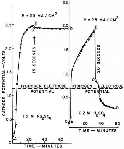
Figure 8 - Dubpernell and Kenney's measurements of cathode potentials on mercury with sodium deposition and with hydrogen evolution.
The two curves in Fig. 8 are shown with the hydrogen electrode potential as a common axis, since this is the zero point or equilibrium potential against which overvoltage is measured. The line AB in each case is the charging curve with gradually increasing current densities up to the maximum shown at B. The circuit is opened at B and the drop in potential followed manually as rapidly as possible from B to C, and then on to D. While with hydrogen evolution in 0.2M H2SO4 there is a sudden drop in potential of about one volt upon opening the circuit, in the case of sodium deposition from 1.5 M Na2SO4 the drop is only about 50 mV at 25 mA/cm2, and the potential is then stable at the reversible sodium deposition potential on mercury. The small drop in potential of about 50 mV is probably largely a measure of the solution IR drop included in the measurement when the current is flowing.
It can readily be noted from Fig. 8 that the overvoltage appears to be identical in the two cases. It seems likely that more refined measurements would only establish the identity more accurately within closer limits. Thus the original idea of overvoltage being due to the electrodeposition of electronegative metal failed to be borne out, but overvoltage instead appears as an intrinsic reproducible property of the cathode metal, mercury in this instance.
The above investigation was checked and extended in 1969-1970 by Kuo-Ming Wu at the University of Detroit67 using the same method and overvoltage on mercury at a given current density appears to be the same whether the cathode process is the deposition of metal from a salt solution or hydrogen evolution from sulfuric acid.
Two main series of measurements were made with two different conductivities of the solutions. The conductivity measurements in each series are shown in Fig. 9, and it is to be noted how closely the conductivities were adjusted.
The first series in Fig. 10 shows the overvoltages at 200 mA/cm2 (200 A/ft2) with cesium, potassium or lithium deposition on the mercury cathode, compared to hydrogen evolution from sulfuric acid. The overvoltages (including IR drop) are essentially identical in each case.
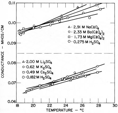
Figure 9 - Kuo Ming Wu's measurements of the conductivity of solutions.

Figure 10 - Kuo Ming Wu's measurements of overvoltage plus IR drop on mercury at 200 mA/cm2.
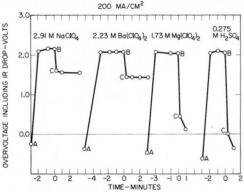
Figure 11 - Another series of measurements by Kuo Ming Wu of overvoltage plus IR drop on mercury at 200 mA/cm2.
The second series in Fig. 11 shows the overvoltage at 200 mA/cm2 (200 A/ft2) in solutions of sodium, barium, and magnesium perchlorate, compared to sulfuric acid of the same conductivity. The sodium and barium deposited with 100% current efficiency with no visible hydrogen evolution; magnesium only deposited at very low efficiency or not at all, but this did not affect the overvoltage measurement. Again the overvoltage (including IR drop) appeared identical in the solutions of the same conductivity, regardless of the exact cathode reaction. The time scale in Figs. 10 and 11 is marked negative during charging, zero at the point of current interruption, and positive when following the decay of potential.
Figures 10 and 11 show typical results; measurements were generally made at 20, 50, 100, 200 and 300 mA/cm2. Over this rather limited range, overvoltage (including IR drop) appeared to vary almost linearly with current density, with the greatest deviation at the lowest current densities. Higher current densities could readily be investigated if the mercury cathode is agitated a little.
The deposition potentials or amalgam potentials of the various metals recorded on open circuit are shown in Figs. 12 and 13, and it is noteworthy that they are quite reproducible and show little variation with current density, considering the fact that the measurements were not of great accuracy and were made more for qualitative than quantitative purposes. The results with magnesium perchlorate are given in Fig. 14, since they also indicate a small open circuit potential due to magnesium deposition.
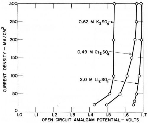
Figure 12 - Open circuit amalgam potentials of lithium, potassium and cesium (Kuo Ming Wu).
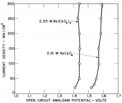
Figure 13 - Open circuit amalgam potentials of sodium and barium (Kuo Ming Wu).
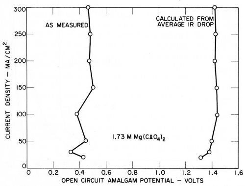
Figure 14 - Open circuit amalgam potentials of magnesium (Kuo Ming Wu).
Some of the indicated IR drops due to the fall in potential on opening the circuit are given in Figs. 15 and 16. Here again, the accuracy of measurement appears to be sufficient for indicative purposes. It was originally thought that only the IR drop through a fixed part of the solution in the cathode chamber would be shown, and that this would be substantially identical in each instance. However, this no longer appears to be the case. Rough calculations indicate that a resistive fall in potential is measured that is substantially larger than would be expected in the cathode chamber solution alone, and the IR drop is greater in the case of solutions giving lower amalgam potentials.
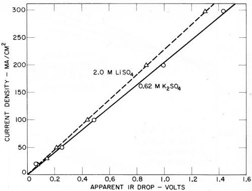
Figure 15 - Apparent total IR drop with potassium and lithium sulfates (Kuo Ming Wu).
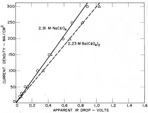
Figure 16 - Apparent total IR drop with sodium and barium perchlorates (Kuo Ming Wu).
The measurements thus indicate that we are dealing with a closed system including its own set of adjustments and balances. There appears to be a powerful force present which regulates the total voltage of open circuit potential and IR drops to a constant amount at a given current density. This is especially evident with the measurements with sulfuric acid solutions, which give a lower total voltage at lower current densities, but which finally increase to match the others as the current density is increased.
It would appear that probably a cell could be designed in which the IR drop in the solution would be accurately known, and thus permit the estimation of any other resistances included in the measurements such as the metallic surface resistance postulated in the present paper.
Discussion
It was first thought66,67 that the apparently reproducible cathode potential called overvoltage was perhaps due to the production of a fixed quantity of hydrated electrons in the solution at the interface corresponding to the current density used. The hydrated electron had been produced and identified by Hart and Boag in 1962,69 by means of pulse radiolysis. This led to a good deal of further investigation of the generation and properties of such hydrated electrons, which culminated in the publication of a separate book on the subject.70
Hydrated electrons, or more broadly, solvated electrons, have an intense blue color and their presence or absence can readily be shown by optical means. It was noted as far back as 187871 that the electrolysis of liquid ammonia turned it blue, but that the liquid became colorless when the current was discontinued. Cady reported in 189772 that the electrolysis of sodium or potassium salts dissolved in liquid ammonia gave a stable blue color which formed at the cathode, and that the resultant solution of sodium, for example, conducted like a metal.
Walker73-76 felt that he detected the formation of hydrated electrons at the cathode in aqueous electrolysis with platinum and silver cathodes by both chemical and optical means, but his results have thus far not been confirmed by more recent work.77
The hydrated electron is a very short-lived species in aqueous solutions, although it is reported to be stable for several milliseconds in alkaline media. In strongly acid solutions it decomposes quite rapidly, and such acid solutions are used as "scavengers" for hydrated electrons.
Since overvoltage (including IR drop) was found to be identical in both acid and in neutral or slightly alkaline solutions, it was concluded that it could not be due to hydrated electrons in contact with the solution at the cathode, and must be located within the metal of the cathode where it would be unaffected by the composition of the solution. This is a startling conclusion requiring extensive revision of one's thinking, but appears to be the only conclusion that fits the facts.
While metal surfaces are commonly considered "homogeneous" right up the final layer of atoms as shown in Fig. 17,78 the surface atoms are obviously stranded in an unbalanced position compared to those in the interior of the metal lattice. They have no choice but to attempt to bond to each other, or to react with or adsorb any gases or liquids that they may come into contact with.
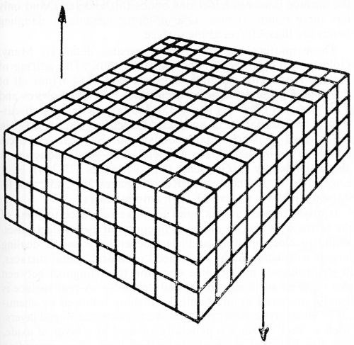
Figure 17 - Rogers' hypothetical crystal of metal containing no dislocations. Reproduced by permission from The Nature of Metals, American Society for Metals, 1964.
The surface tension of metals and other solids is thus quite high, ranging roughly from 10 to 100 times that of aqueous solutions containing various concentrations of wetting agent.79,80
Desch79 gives the surface tension of ordinary salt, NaCl, as 3000 dynes/cm. Zwicky81 reviews the necessity of microscopic cracks in the surface of even the most perfect crystals, such as NaCl crystals, for example. The lattice spacing on the surface of such NaCl crystals is about 6% smaller than the spacing in the solid crystal, resulting in a tendency for the surface to contract. Zwicky's drawing of the probable cross section of the surface of an NaCl crystal is shown in Fig. 18. He considers that the surface is probably broken up into blocks consisting of about 10,000 atoms each.
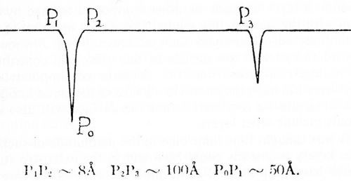
Figure 18 - Zwicky's concept of the surface structure of a crystal of sodium chloride.
These considerations are borne out by the low breaking strength of NaCl crystals, about 50 kg/cm2. If the surface is wetted, however, it will stand stresses as high as 16,000 kg/ cm2, near the theoretical value.
Such behavior is not uncommon. Thus chromium is a brittle metal, and much effort has been expended to produce it in ductile form.82 The writer at one time received a sample of Bureau of Mines' chromium wire the size of an ordinary paper clip when opened out. This chromium wire was stronger than the steel wire in bending, and could withstand almost any amount of bending. An important feature of making such chromium is the final removal of any air contaminated layer on the surface, and the effects of any notches, by electropolishing as the last stage of production (Ref. 82, pages 138-162).
This question of the breaking strength of crystals and the mosaic structure of their surfaces was discussed in 1933 in a German physics handbook (Ref. 83, pages 765-770). A good deal of work along this line was done by Adolf Smekal, who contributes a long chapter on the structure-sensitive properties of crystals to the same handbook (Ref. 83, pages 795-922). Desch also has a chapter on mosaic structures in crystals (Ref. 79, pages 77-87).
More recently, some discussion of mosaic structure on the surface of metal crystals is to be found,84,85 but the emphasis has shifted to imperfections distributed throughout the whole crystal rather than to surface studies. Hirsch85 retains the term "mosaic" for crystals which really do consist of slightly misoriented blocks, but devotes most of his attention to the distribution of dislocations in bulk metals. Figure 19 copied from Hirsch's review shows a theoretical cross-section of a block of metal from Buerger,86 showing the way he considers metal crystals to grow into what he calls a "lineage" structure, but without particular reference to the final structure of the surface of the metal.

Figure 19 - Buerger's concept of a "lineage" structure of the cross section of a metal crystal. Reprinted with permission from Pergamon Press Ltd.
Adsorption on metal surfaces has been extensively studied, but it is not clear whether the first layer of molecules strongly adsorbed ("chemisorbed") on the surface can be considered to be part of the solid, or whether they still have some association with the solution, de Boer" found that the heat of adsorption is higher in capillaries than on flat surfaces, and that adsorption in such pockets, holes and cavities accounts for the experimentally known values of the heat of adsorption. Figure 20 is his sketch of adsorption within a capillary extending from right to left (Ref. 87, page 212). The line SS is the surface of the solid with the actual surface atoms indicated. The row of molecules aa is the first layer adsorbed, bb is the second, cc the third and dd the beginning of a fourth layer. Adsorption has sometimes been used to estimate the true area of a metal surface, since it is to a considerable extent a reversible process.
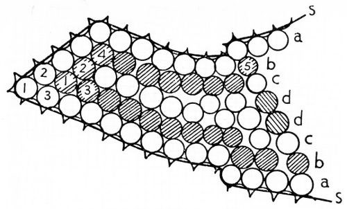
Figure 20 - deBoer's diagram of adsorbed layers filling a crevice in a solid surface. Reprinted by permission from The Clarendon Press, Oxford.
The surfaces of semiconductors such as germanium and silicon have been studied extensively in recent years in view of their use in device technology. There seems little reason to suppose that metal surfaces are radically different, and much of what is learned regarding semiconductor surfaces should also apply to metals. In fact, metals are ordinarily exposed to air and aqueous solutions and ordinarily have a surface layer of oxide on them which is in itself usually a semi-conductor.
Thus, bright metallic chromium was found by Andreeva88 to form a "natural" oxide film on its surface 10-20 Å thick as soon as it was exposed to air at 25°C, and this oxide film thickened to 25-35 Å within 24-48 hr, after which it remained constant. This oxide film is normally invisible. Bright chromium plate is deposited with a varying thickness of oxide on it, sometimes so thick that it is visible. Holliday and Frankenthal89 found about a 10 Å thick chromium oxide layer on a 50 Å thick chromium plate by chemical analysis.
D. R. Turner (Ref. 90, pages 285-310) considers that electrochemical reactions on metals may be characterized by phenomena occurring in the solution, but that if the electrode is a semiconductor, the rate determining process may also include phenomena that take place inside the surface of the electrode. In the study of germanium, he considers that each surface atom is covalently bonded on the average to two underlying germanium atoms. Current multiplication results are assumed to be associated with the "dangling-bond" electrons that remain on the underlying germanium atoms after the surface atom goes into solution during anodic action.
The electrical properties of the surfaces of semiconductors are also well reviewed by P. Handler (Ref. 90, pages 54-68). Handler considers that the surface region may consist of only the first layer of atoms or perhaps the first few layers of atoms. The existence of "surface states" equal to the number of surface atoms is discussed, and it is felt that these surface states may extend to the subsurface atoms. A germanium atom at the surface does not have four bonds to the crystal, and only has three bonds at best. One or more orbitals or dangling bonds are thus left free at the surface.
These matters are discussed in greater detail by Many, Goldstein and Grover,91 who conclude that "The pairing of surface atoms, for example, suggests that most if not all of the dangling bonds saturate each other." F. M. Fowkes and T. E. Burgess (Ref. 92, pages 351-360) give a detailed discussion of the formation of an internal electrical double layer in the surface of silicon oxide on silicon. Such an electrical double layer in the surface of metals and semiconductors is also discussed by H. Gerischer (Ref. 90, pages 177-204), H. J. Engell and K. Bohnenkamp (Ref. 90, pages 225-243), and R. Parsons (Ref. 93, pages 103-179), among others.
It might be well at this point to make reference to some of the terms with special meaning in common use in electronics. While in electroplating and electrochemistry one is dealing largely with what might be termed "ordinary" metal surfaces, in electronics it has become common to distinguish between two types of surfaces, "real" and "clean."94 A real surface is usually prepared by mechanical polishing followed by chemical or electrolytic etching to remove the outer damaged layers. Such a "real" surface is generally covered by a layer of oxide, and also by other molecules adsorbed from the surrounding media. The "real" surface is not particularly different from a surface prepared for plating, but the operations are more precise and clearly defined, and carried out with greater care.
"Clean" surfaces are produced and maintained in an ultrahigh vacuum (10-10 to 10-8 mm Hg), by cleavage, by ion bombardment, or by heating at a high temperature in the vacuum. In this way surfaces are obtained and maintained that have something of a theoretical quality and are free of foreign adsorbed matter to better than a few per cent of an atomic monolayer. Nevertheless, such "clean" surfaces are said94 to commonly exhibit lattice spacings twice as large as those in the bulk, and more complex structures are also observed.
Conduction in semiconductors is considered to be of two types, n-type (negative) and p-type (positive). Certain impurities (donors) give rise to n-type conduction, in which the electrons are the majority carriers and holes (positive, and otherwise similar to an electron) are the minority carriers. Other impurities (acceptors) result in p-type conduction in which the holes are the majority carriers and the electrons the minority carriers. We might say that there are two types of electricity, positive and negative, holes and electrons.
On the basis of these discussions it is proposed that metal surfaces are covered by a higher resistance layer of molecules of metal, probably at least several molecules thick, as shown in Fig. 21, or some equivalent. The presence of such a layer seems necessary to account for the potential difference called overvoltage, which seems to be located in the surface of the metal and to be a property of the metal itself. This overvoltage could not vary with current density if the metal was a uniform good conductor right up to and including its surface atoms.
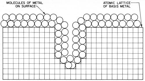
Figure 21 - Suggested diagram of the cross-section of metal showing the proposed layer of “molecular metal” on the surfaces.
Such a surface layer of "molecular metal" could hardly be expected to exist by itself under ordinary circumstances; and in contact with air and water, for example, would also have to include a layer of oxide or other compound formed by reaction with the surrounding media. It is also a question to what extent any adsorbed layers such as shown in Fig. 20 should be considered part of the surface of the solid, and contributing to its electrical properties. For the sake of simplicity, only one layer has been shown on the surface of the metal in Fig. 21, but it should be considered that the surface will also commonly include other layers.
It was thought that some clue to the magnitude of such surface layers on metals could be found in the extensive studies which have been made of thin films. This should be true particularly of gold, which has outstanding surface properties. Unfortunately, this does not work out in the investigations made to date, since the thin films have to be deposited on a substrate by electrodeposition, by evaporation, or by cathode sputtering in a vacuum, and the substrate seems to control the nature of the first few layers of atoms deposited.
Figure 22 (Ref. 94, pages 373-381, chapter by K. L. Chopra and L. C. Bobb on "Electrical Conduction In Thin Epitaxially Grown Gold Films") shows that even the most carefully sputtered gold films tend to have a high resistivity when the thickness goes below 200 Å. This is confirmed by Prostak, Mark and Hansen,95 who state that a gold film thinner than about 200 Å evaporated onto glass is a very high resistance deposit which has a bluish color in transmitted light. These workers were able to obtain gold films of medium resistance by other means down to a thickness of about 50 Å, but thinner films had an extremely high electrical resistance. A comprehensive review of size-dependent electrical conduction in thin metal films and wires by D. C. Larson is available (Ref. 96, pages 81-149).
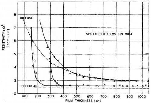
Figure 22 - Chopra and Bobb’s measurements of the resistivity of sputtered polycrystalline and single-crystal (left hand curve) gold films on mica. Reprinted with permission from Pergamon Press Ltd.
Chopra97 showed very clearly by means of transmission electron micrographs, the exact manner in which the thinner gold films less than 100 Å thick are made up of islands, and not a continuous film at all. As the film thickens or is heat treated, electrical continuity is attained at a critical thickness, and coalescence of the islands is also seen to occur as would be expected.
A current review98 of the surface structure of gold indicates that the anomalous nature of the first two or three atomic layers is still incompletely understood.
There has been a good deal of investigation recently of optical phenomena at electrodes during electrochemical reactions, which may be considered under the title "electroreflectance" (ER). Kuwana published99 an extensive review which includes the comment that: "In the double layer region, the ER due to the solution side of the interface appears to be small compared to ER of the metal surface, assuming specific adsorption is absent."
Another area which will benefit from the theory proposed here is that of the cathodic electrolytic heating of metal surfaces. There is a long bibliography on this subject extending all the way back to Sir Humphry Davy in 1808. Briefly, if a metal surface is made cathode at a high current density such as 3 to 5 A/cm2 using 100 to 300 Vdc and a solution such as 5 to 10% sodium carbonate, there is arcing at the surface, which is heated red hot and even to melting. Iron and small platinum wires can be melted in this way. The process has been used commercially for case hardening in half a dozen countries, but does not seem to have achieved a noteworthy industrial importance. It is an excellent means of heating a metal surface, and it is helpful to think of the heat being generated in the surface of the metal directly, as well as in an arc against the solution. Reference is made to a book by Yasnogorodski100 and to three German articles by Eichhorn.101-103
Related Content
How to Maximize Nickel Plating Performance
The advantages of boric acid-free nickel plating include allowing manufacturers who utilize nickel plating to keep up the ever-changing regulatory policies and support sustainability efforts.
Read MoreSuccessful South African Plater Beating the Odds
Remaining focused on quality and reliability, Team Plating Works stays profitable in a volatile and challenging economy.
Read MoreAn Overview of Electroless Nickel Plating
By definition, electroless plating is metal deposition by a controlled chemical reaction.
Read MoreTroubleshooting Alkaline Zinc
One of the most common problems that can arise when plating with alkaline zinc is an imbalance of brightener in the solution. In this helpful Ask the Expert article, Chad Murphy of Columbia Chemical discusses how different zinc metal concentrations and brightener concentrations can impact efficiency.
Read MoreRead Next
A ‘Clean’ Agenda Offers Unique Presentations in Chicago
The 2024 Parts Cleaning Conference, co-located with the International Manufacturing Technology Show, includes presentations by several speakers who are new to the conference and topics that have not been covered in past editions of this event.
Read MoreEducation Bringing Cleaning to Machining
Debuting new speakers and cleaning technology content during this half-day workshop co-located with IMTS 2024.
Read MoreDelivering Increased Benefits to Greenhouse Films
Baystar's Borstar technology is helping customers deliver better, more reliable production methods to greenhouse agriculture.
Read More


.jpg;maxWidth=300;quality=90)


