Electroplating of Carbon Nanotube Yarns and Tapes with Five Metals
Carbon nanotube (CNT) tapes and yarns can reduce the weight of industrial cables for aviation and space by substituting for copper. In order to attach CNTs to connectors, one high-reliability method of attachment is soldering, which is difficult; however it can be facilitated by electroplating. In this study, CNT tapes and yarns were plated with Cu, Ag, Ni, Sn and Au.
by
Mike Sereda*
Materion Large Area Coatings
Windsor, Connecticut, USA
Editor's Note: A printable PDF version is available by clicking HERE.
ABSTRACT
Carbon nanotube (CNT) tapes and yarns can reduce the weight of industrial cables for aviation and space by substituting for copper. In order to attach the CNTs to cable connectors, one high-reliability method of attachment is soldering. Soldering to CNTs is extremely difficult; however it is facilitated by electroplating the CNT with solderable metals. In this study, CNT tapes and yarns were electroplated with copper, silver, nickel, tin and gold. Electrodeposition rates of CNT yarns were 5.5, 3.9, 6.7, 19.9, and 0.64 μm/min, on copper, silver, nickel, tin and gold, and on CNT tapes similar numbers scaled down by area. Best surface treatment, current, loading, temperature, concentration, additives, correct anode, and their effect on efficiency, deposition rate and adhesion were determined. Adhesion of copper films improved markedly over 15 μm thickness. Multiple samples of up to five at a time were deposited by scaling up the current by the number of samples. The Cp value was 3.4 for copper, indicating copper plating was repeatable.
Keywords: CNT, carbon nanotube, electroplating, adhesion, SPC, current efficiency, soldering, attachment.
Introduction
Carbon nanotubes (CNTs) are a widely studied allotrope of carbon. Their size-to-length ratio creates unique physical properties, such as tensile strength and conductivity, which outperform common bulk materials. Possible applications of CNTs are energy storage, interconnects for CMOS and sensors.1 Military and commercial aircraft and satellites have miles of cable that are used for transmitting signals and power. Carbon nanotube (CNT) tapes and yarns are lightweight conductive materials that show potential for signal and current carrying capacity. These light-weight materials could enable military and commercial aircraft and satellites to travel further on less fuel. By replacing copper in a cable with CNT materials, the weight of a cable assembly can be reduced 70%.2 While mechanical crimps are an adequate termination strategy, soldering directly onto the CNT materials is not possible due to their hydrophobicity.3,4 By metallizing the CNT via electroplating and/or electroless plating metals, soldering is possible. TE Connectivity** is researching the replacement of copper in cable assemblies, and has already used CNTs for USB cables.
Theory
Discovery and demonstration
The first mention of a carbon filament from the decomposition of methane is credited to Edison in 1889 in an electric light bulb patent.5 The first TEM image of tubular carbon filaments was published in Russian (Fig. 1).6 Iijima7 is given credit for demonstrating the presence of CNTs in the cathode arc in electric arc trials intended to create fullerenes (C60). A survey article of the history of carbon nanotubes, graphene and fullerenes appeared in Carbon in 2006.6 The authors discuss the almost simultaneous identification of single-walled CNTs (SWCNTs) at IBM by Bethune8 in 1993, and Iijima and Ichihashi,7 published a month earlier.
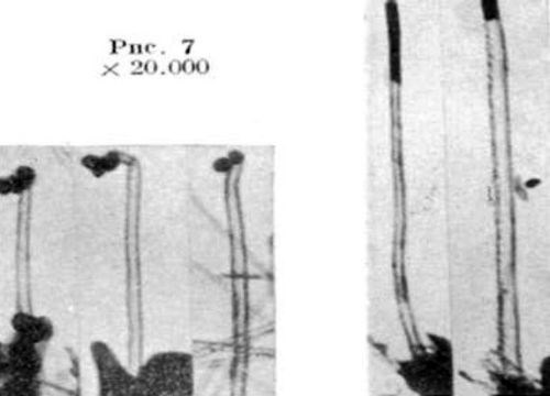
Figure 1 - First TEM of a CNT, multi-walled6 (reprinted with permission).
Structure
Anantram and Leonard9 studied the structure of CNTs. They found armchair, zigzag and chiral structures. The multiwall carbon nanotube structure consists of multiple single-wall CNTs (SWCNTs) inside each other like a Russian doll, with the interplanar distance being similar to the interplanar distance of graphite. With no dangling bonds, each carbon atom is bonded to three nearest neighbors, all sp2-double bonded. Although the conduction mechanism is complex in large-format CNTs (tapes and yarns), SWCNT and MWCNT (multiwall CNT) exhibit exclusively metallic conduction in armchair, and either metallic or semiconducting conduction in zigzag and chiral configurations (Fig. 2).
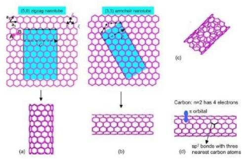
Figure 2 - (a) Zigzag carbon nanotube, (b) armchair and (c) chiral structures9 (reprinted with permission).
Functionalization
Carbon nanotubes can be modified to contain R-COOH groups when treated in nitric and sulfuric acid,9 according to theory. Moreover, 1-3% of the carbon atoms are at defective five-carbon rings, known as Stone-Wales defects, as shown in Fig. 3, where chemical attachment can occur.9 Thermal oxidation can produce the aforementioned R-COOH group, as shown in Fig. 4.10 Rafieem, et al.11 modified the surface of graphene to obtain hydrophilic (wetting) graphene by sonicating in water, and hydrophobic by sonicating in acetone. Oxidation and plasma activation can also modify this property,11 as well as amidization. Basiuk, et al.12 treated carbon nanotubes with amine vapor at 170°C in reduced pressure to amidize the R-COOH group.
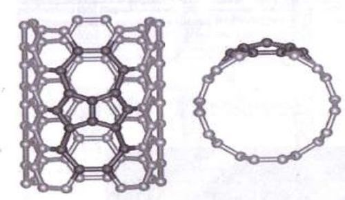
Figure 3 - Stone-Wales defects (five-rings)10 (reprinted with permission).
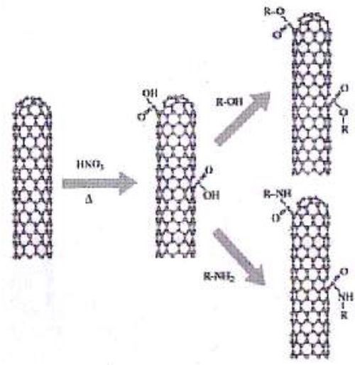
Figure 4 - Thermal oxidation (delta), with acid treatment in nitric acid, followed by esterification or amidization10 (reprinted with permission).
Since the C=C bonds in CNTs are not reactive, the R-COOH molecules are reactive groups which could be used for attaching plating metal ions after reduction. Balasubramanian found that for functional groups, Raman peaks for radial breathing mode intensity increased, indicating hexagonal lattice disturbance; and the D-or disorder peak also increased in intensity.10 Atomic force microscopy (AFM) confirmed the existence of the functional group. It is by activation of these functional groups that electroplating should occur, by means of preclean and chemical functionalization in the plating solution.
Experimental
Wetting angles were measured with the Rame-Hart drop angle tester. The cleaning procedure was then executed in two steps, one for degreasing and one for cleaning. Tapes/yarns were then subjected to various chemicals commonly found in electroplating and electroless plating. Selection of parameters and their values, as well as chemical mixtures and conditions, were made iteratively based upon results.
Results and discussion
Summary
Continuous, adherent films were demonstrated with commonly available chemicals from plating suppliers. Multiple tapes and/or yarns were plated, simultaneously, electrolytically or electrolessly. In electroplating all tapes/yarns need to be connected to the cathode in parallel. In electroless plating, the rate depends upon total amount of surface area and chemistry. In an industrial process, ideally hundreds of tapes/yarns might be plated at the same time. This is because tapes/yarns only need to be plated on the ends for soldering. CNTs have one ohm/inch resistivity presently, and by embedding metals will eventually lead to much lower resistivity.
Plating results
Electroplated tapes and yarns are shown in Fig. 5. SEM cross sections are shown in Figs. 6 and 7. As expected, metal area had bright appearance under backscattered electrons due to higher electron fluorescence, while carbon nanotube and potting compound appear dark. The black square indicates an analysis spot (plated metal) for SEM. The electrodeposition rates are shown in Fig. 8.
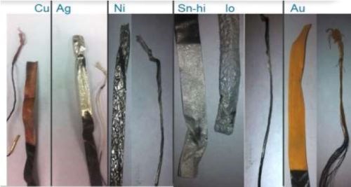
Figure 5 - Carbon nanotube tapes and yarns, electroplated with (L-R): Copper, silver, nickel, tin with high concentration, tin with low concentration, and gold. The plated area is approximately 4 in. (10 cm) long.
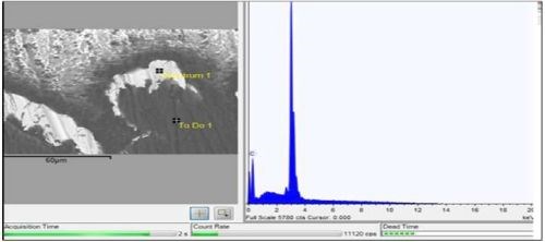
Figure 6 - Backscatter SEM and EDX of silver cross-section (Square).
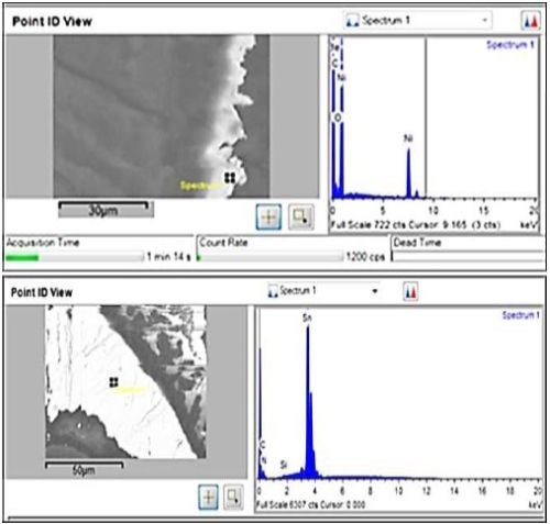
Figure 7 - Backscatter SEM and EDX of nickel cross-section (top); tin (bottom).
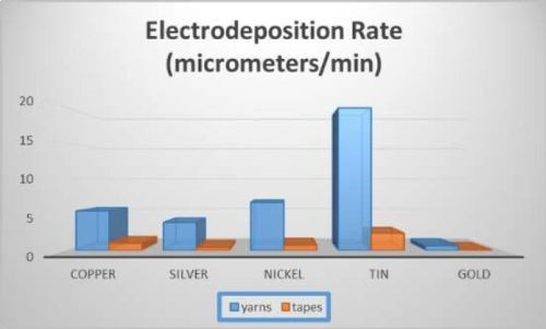
Figure 8 - Electrodeposition rates.
Wetting and adhesion
Pre-plating wetting can be tested by contact angle. Hydrophobic surfaces produce a higher contact angle in a liquid, hydrophilic a lower angle. Yarns/tapes were cleaned in a two-step process. This treatment caused the yarns/tapes to degrease (increased contact angle) then wet (decreased contact angle). Acetone was used to degrease, 10% sulfuric acid to wet. For basic plating solution (silver), KOH was substituted for sulfuric.
Adhesion was tested on tapes using ASTM D3359, using a crosscut kit. Figure 9 shows that for copper-nickel (nickel plated over copper) and copper, adhesion was excellent. Yarns were penetrated by the metal, shown in SEM in Fig. 10, indicating adhesion was also excellent.
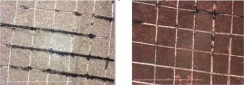
Figure 9 - ASTM D3359 passing samples. Note the lack of missing material. Cu-Ni 4; Cu 5 (5 is ideal).
Development of deposition conditions
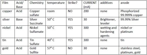
Deposition conditions were developed iteratively with thickness results. Variables that were evaluated were: type of substrate (yarn or tape), anode type, current, one-or two-step deposition, number of samples (loading), temperature, and concentration of acid. Early in experimentation stirring was eliminated as a variable because stirred electroplated solutions did not adhere, presumably because nucleation was too slow. Multiple step depositions were required for silver, tin and nickel. Silver was found to require a different concentration acid in the first step. These multiple step depositions are referred to as strike and deposit. Plating solutions and conditions are found in Table 1.
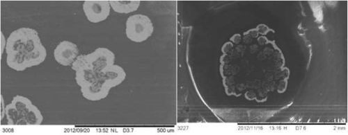
Figure 10 - Left: Copper yarn. Each yarn is penetrated. Right: Tin yarn. The periphery of the yarn bundle had coating at the edge. In both samples, the thickness measured to be 60 μm. In the backscatter SEM, the metal appears as bright, potting compound and CNT as dark.
Table 1 - Plating conditions.
Multilayer films
Five film combinations were successfully deposited in layers: Cu-Ni-Sn, Cu-Ni-Au, Cu-Ni-Ag, Cu-Ni, Cu-Sn, and Cu-Ag (Fig. 11). At the onset of copper deposition, Cu-Ag had to be dipped into the silver plating solution with the current on to avoid the copper dissolving in the basic silver plating solution.
Multilayer films were intended to solder better than single layer films, e.g., CuNiSn, a common solder film. Nickel is a diffusion barrier between copper and tin. Used in solder bump for silicon-metal bond pads, copper sticks to the surface of the soldered item, and tin interacts metallurgically with solder. Cross-section SEMs (Fig. 12) of multilayer films showed there was no layer structure. This is explained by the porous open nature of carbon nanotube macrostructure, in which a film might deposit anywhere in the volume not necessarily on top of the previous film. Therefore single layer structures would be preferred.
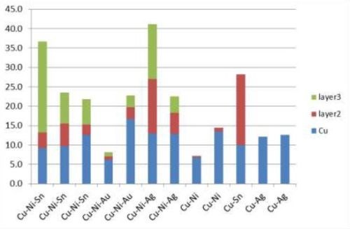
Figure 11 - Thicknesses of multilayer films.
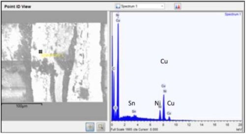
Figure 12 - Copper, nickel and tin in same location, therefore no layers.
Repeatability
The calculation of weight gain/minute allows yarn and tape data to be combined. The average, standard deviation and standard deviation/average for electroplated films, are shown in Table 2.
Copper had a Cp of 3.4 which is extremely high. Cp is a measure of process repeatability13
as defined in Equation 1:
(1)
The specification range defines what is expected in range, that is, upper limit-lower limit. The purpose of these films is to solder to connectors, therefore a wide range would be expected. LSL is the lower specification limit; USL is upper limit. The copper SPC control chart is shown in Fig. 13.
Table 2 - Deposition rate (average value) of films in mg/minute; standard deviation and standard deviation /average; population (number of samples).

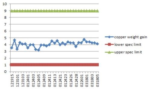
Figure 13 - Copper SPC control chart.
Development of thinner films
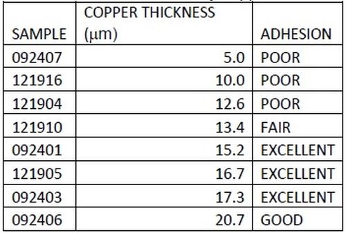
As outlined earlier, adhesion was excellent. Figure 14 shows a top-down backscatter SEM of a copper sample, with 5 μm of copper film. As shown in Table 3, adhesion suffers for films of less than 10 μm. To save on materials, time and cost, all industrial processes seek to optimize parameters, in this case lower thickness. To this end, adhesion of copper was tested at different thicknesses. A top down SEM (Fig. 14) shows that copper coverage below a 5 μm thickness is not continuous on a microscale. Films above 10 μm were continuous.
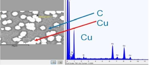
Figure 14 - Top down backscatter SEM, and EDX of copper region, for 5 μm thick film.
Table 3 - Adhesion results by copper thickness, showing that a 15 μm thickness showed good adhesion.
Current efficiency
One measure of quality of plating is the current efficiency. Originally developed by Michael Faraday,14 current efficiency was used to confirm that plating results are theoretically justified. Current, weight gain and time are related by equation 2:
(2)
If the efficiency is less than 25% or more than 100%, the results are suspect. Current efficiency was highest for copper, followed by nickel, silver, tin and gold (Fig. 15). The efficiency (average of all readings) for copper, silver and nickel was near 1, as expected by theory, but tin and gold were below 1.
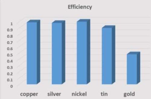
Figure 15 - Efficiency (average value) of films.
Electroless plating
Based on the SEM results in Fig. 14, an attempt was made to increase the density of nucleation sites for copper electroplating by electroless copper plating. This would allow for electroplated layers thinner than 10 μm to adhere well.
Seven of 22 samples were electrolessly plated successfully, a yield of 31.8%. These samples were pink and conductive. Weight gain varied from 0.2 to 2.1 mg/min, which converts to 0.4 to 1.2 μm/min, a thickness range of 2.0 to 23.6 μm. Paradoxically, there were samples with as much weight gain (that did not change color) that did not apparently have copper. The lack of copper was confirmed using EDX. This result did not occur with the electroplating results, which were all affirmative for samples with weight gain. No electroplated samples had weight gain without color change or EDX verification of the plated film. Unlike the electroplating results, the weight gain did not correlate with copper color. Possible causes for film deposition not being repeatable are the surface treatment by 10% sulfuric acid not being aggressive enough (boiling may be needed or other treatment needed - nitric acid14); sensitizing by palladium and tin not being effective or sufficient, possibly due to low temperature; and contamination of the copper plating solution. Further study will be required to elucidate these mechanisms so that thinner layers of copper can be used for solder connectors.
Conclusions
Using commonly available plating chemicals, carbon nanotube tapes and yarns were plated with copper, silver, nickel, tin and gold. Adhesion was excellent. These plated films will aid in the development of aircraft and space cable assemblies by enabling attachment mechanisms for CNTs, which replace copper and save on weight to extend flight range.
Acknowledgements
This research was done under the sponsorship of TE Connectivity (Menlo Park, CA) and San Jose State University (San Jose, CA), in Mike Sereda’s Masters project. Special thanks is given to the Advanced Development Group under Stefanie Harvey for sponsoring the work, and to Jeanine Olson for editing.
References
1. Y. Zhou, “Carbon Nanotube Synthesis on CMOS Substrate via localized Resistive Heating,” Ph.D. thesis, University of Florida, (2009).
2. S. Harvey, “Carbon as Conductor: a Pragmatic View,” https://escies.org/download/webDocumentFile?id=62169; last accessed 02-02-2016; downloads a pdf file.
3. Z. Wang, et al., Nano Letters, 7 (3), 697-702 (2007).
4. Y Tseng, et al., New Diamond and Frontier: Carbon Tech., 14 (3), 193-201 (2004).
5. T. Edison, U.S. Patent 223,898 (1890).
6. M. Monthioux & V.L. Kuznetsov, Carbon, 44 (9), 1621-1623 (2006).
7. S. Iijima & T. Ichihashi, Nature, 363, 603-605 (1993).
8. D.S Bethune, et al., Nature, 363, 605-607 (1993).
9. M.P. Anantram & F. Léonard, Rep. Prog. Physics, 69 (3), 507-561 (2006).
10. K. Balasubramanian and M. Burgard, Small, 1, 180-192 (2005); http://tinhoahoc.com/Nanotechnology/C-nanotube-Small02-2005.pdf; last accessed 02-02-2016.
11. J. Rafiee, et al., Adv. Mater., 22 (19), 2151–2154 (2010).
12. E.V. Basiuk, et al., J. Phys. Chem. B, 106 (7), 1588-1597 (2002).
13. D.C. Montgomery, Introduction to Statistical Quality Control, John Wiley and Sons, 2005.
14. X. Chen, et al., Composites Sci. Technol., 60 (2), 301-306 (2000).
Footnotes:
*Corresponding author:
Mike Serada
PVD Engineer
Materion Large Area Coatings
300 Lamberton Road
Windsor, CT
Phone: (860) 688-2300; Ext. 646
E-mail: Mike.sereda@alum.mit.edu.
**TE Connectivity, Menlo Park, CA.
About the author

Related Content
Liquid Chrome Vs. Chromic Acid Flake
Contemplating how to continue offering chromic acid services in an increasingly stringent regulatory world? Liquid chrome products may be the solution you’re looking for.
Read MoreInnovation in Plating on Plastic
Plating on advanced plastics solution offers improved adhesion, temperature resistance and cost savings.
Read MoreAdvantages to Pumped Eductor Agitation
Not all agitation methods are created equally. Pumped agitation with eductor nozzles can improve process tanks and quickly show a reduction in operating costs while keeping staff safe, following environmental legislation and preventing pollution.
Read MoreAn Overview of Electroless Nickel Plating
By definition, electroless plating is metal deposition by a controlled chemical reaction.
Read MoreRead Next
Episode 45: An Interview with Chandler Mancuso, MacDermid Envio Solutions
Chandler Mancuso, technical director with MacDermid Envio discusses updating your wastewater treatment system and implementing materials recycling solutions to increase efficiencies, control costs and reduce environmental impact.
Read MoreDelivering Increased Benefits to Greenhouse Films
Baystar's Borstar technology is helping customers deliver better, more reliable production methods to greenhouse agriculture.
Read MoreEducation Bringing Cleaning to Machining
Debuting new speakers and cleaning technology content during this half-day workshop co-located with IMTS 2024.
Read More






.jpg;maxWidth=300;quality=90)
