Methods and Formulas to Determine Internal Deposit Stress in Applied Metallic Coatings
Internal stress exists in electroplated and chemically applied metallic coatings. This paper reviews the test procedures for measuring deposit stress and the formulas used to calculate stress values. Many formulas used require modification to obtain actual internal stress values. Errors in this regard are examined and common mistakes are explained.
by Frank Leaman, Specialty Testing and Development Company, York, Pennsylvania, USA
Editor’s Note: This paper is a peer-reviewed and edited version of a presentation delivered at NASF SUR/FIN 2014 in Cleveland, Ohio on June 10, 2014. A printable PDF version is available by clicking HERE.
ABSTRACT
Internal stress exists as an inherent force within electroplated and chemically applied metallic coatings. This induced stress can be tensile or compressive in nature, causing the deposit to contract or expand in relation to the base material. High levels of stress in deposits produce micro-cracking and macro-cracking in the applied layers, and in severe cases produce a lack of deposit adhesion in the form of blistering, peeling and flaking, wave-like ripples in electroforms, and accelerated corrosion and wear failure. This paper reviews the methods and test procedures for measuring deposit stress and the formulas employed for calculating stress values. Many of the formulas used to calculate deposit stress require modification to obtain the actual internal stress value. Errors in this regard are examined and common mistakes in test methods and practice are explained.
Keywords: internal stress, metallic coatings, coating stress, stress measurement, sulfamate nickel
Introduction
Internal stress exists as an inherent force within electroplated and chemically applied metallic deposits. This induced stress can be tensile or compressive in nature, causing the deposit to contract or expand in relation to the base material. High levels of stress in deposits produce micro-cracking and macro-cracking, and in severe cases produce a lack of deposit adhesion in the form of blistering, peeling and flaking. In extreme cases, wave-like ripples in electroforms, accelerated corrosion and deposit wear failure can also occur.
This paper reviews test methods, procedures and formulas used to determine the internal stress in applied metallic coatings. A comparative study for the determination of internal tensile deposit stress as plated from a semi-bright sulfamate nickel plating electrolyte was completed for the Spiral Contractometer Method and for the Deposit Stress Analyzer Bent Strip Method. Spirals were used in this study to compare the former style contractometer design and the recently designed style with and without a masked surface on the spiral inside diameter. Also, the formulas that are frequently used to calculate deposit stress values in applied metallic layers were evaluated. Limitations of these formulations, accuracy of the results and frequent errors in their use are also reported.
Two primary ways that are in use worldwide to evaluate internal deposit stress in metallic coatings are the spiral contractometer and the bent strip methods. The spiral contractometer test procedure is defined in the American Society for Testing Metals Standard B636–84. The bent strip method referred to as the Deposit Stress Analyzer method is currently in the final step of qualification to become an ASTM Standard. Each of these test procedures is applicable for determining both tensile and compressive stressed deposits. Several other test methods have been used in the past, but these have not been put into common practice. The stress meter makes use of a disk that bows inward or outward as deposition commences depending on the nature of the stressed deposit. Accuracy and stripping metal deposits from the disk remain problematic. Another method to determine deposit stress is based on measuring the change in the length of a substrate material that is caused by stress within an applied metallic coating. This method yields consistent results, but the equipment set-up is complicated and there has never been a manufacturing source for its use.
Spiral contractometer
The spiral contractometer method uses a stainless steel spiral having a surface area of approximately 13 in2 (33 cm2) as the test piece. In the test procedure, the upper end of the spiral is held in a stationary position while the lower end is free to rotate as deposition of a stressed coating is applied. Induced stress that is compressive in nature will cause a spiral to contract by winding tighter, while a tensile stressed coating will cause a spiral to unwind. This movement is transferred to a dial measurement disk that is free to move at the top of the contractometer around a measurement scale that displays the spiral movement in degrees as it occurs (Fig. 1).
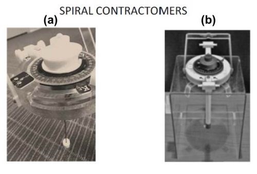
Figure 1 - Spiral contractometer designs: (a) Prior design; (b) New design.
In the prior contractometer design (Fig. 1a), a spiral is supported by a stainless steel center rod in a geometry that allows significant metallic deposition to occur on the inside spiral surface when not protected by a masked coating during a given test. The calculated internal deposit stress result can be in error by as much as 30%, depending on the deposit being evaluated. A common practice is to cover the interior spiral surface with a mask material prior to its use to prevent plating on the interior surface.
A recently designed spiral contractometer (Fig. 1b) improves this geometry problem by surrounding the center supporting rod with a non-conductive glass filled nylon material that occupies almost all of the interior open space so as to discourage deposition of metal on the interior of a spiral during the plating period. This new design also allows the mounting of a spiral in a way that allows plating of the outside surface of a spiral entirely from tip to tip. Since every spiral has exactly the same plated surface area, an estimated surface area calculation that becomes a best guess effort is no longer necessary. Also, construction of these spirals from thinner stock material yields shorter test times for a given set of plating parameters. The recently designed spirals are constructed from 0.010-inch thick stainless steel and have a precise surface area of 13.57 in2. The recommended average test deposit thickness is 500 µ-in (12.7 µm).
Bent strip test
The deposit stress analyzer method for internal deposit stress determinations is based on a bent strip technique wherein the applied metallic deposit induces movement of a base material to an extent that permits a measurement reading over an incremented scale (Fig. 2a). This procedure utilizes pre-calibrated test strips that have a plated surface area of 1.2 in.2 (3.05 cm2) and are intended for a single measurement. As a stressed coating is applied to a test strip, the divided part of the test strip separates so as to allow a measurement of the movement in units at the tips of the divided area (Fig. 2b). Test strips are supplied in a pre-calibrated state. A typical plating test time is 2-4 minutes.
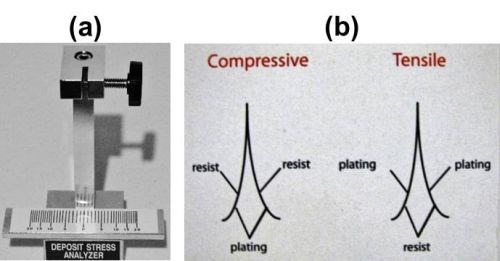
Figure 2 - Bent strip method: (a) test stand and scale; (b) deposit stress configurations on a test strip.
The deposit stress analyzer method features a diversity of test cell geometries for lab bench and in tank use. The In-site 1 plating cell can be used in a solution volume as small as 400 mL (Fig. 3a). This is a great advantage when testing the internal stress of precious metal deposits or when conducting tests to determine the results of incremental additions to a plating bath sample. Larger plating cells utilize a pump for agitation and an immersion heater for use on a laboratory table (Fig. 3b).
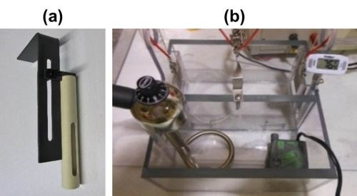
Figure 3 - (a) In-site 1 cell; (b) test cell with accessories.
Bent strip and spiral contractometer compared
For the comparative evaluations of the bent strip and spiral contractometer methods that follow, a semi-bright nickel sulfamate plating bath was used that produced tensile stressed deposits. The results for these test methods are as follows.
Bent strip method
A. Plating conditions for Cu-Fe alloy test strips 0.002 in. thick:
- Plate each test strip at 0.25 A, 30 A/ft2, 3 min at 140 ± 1°F for a target deposit thickness of 75 µ-in.
B. Results (for three samples):
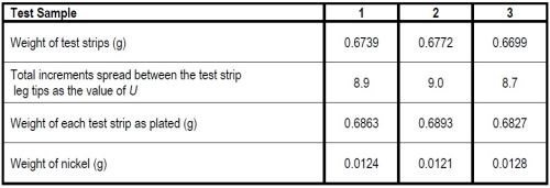
C. Calculation of the deposit thickness:
1. Formula for deposit thickness:
where
T = Average deposit thickness (in.),
W = Deposit weight (g) and
D = Specific gravity of the deposited metal (g/cm3).
2. Deposit thickness:

D. Calculation of deposit stress:
1. Formula to calculate deposit stress follows:
where
S = Internal deposit stress (PSI),
U = Total number of increments spread,
K = Test strip calibration constant,
M = Modulus of elasticity of deposit ÷ that of the substrate
= 1.714 for nickel deposits over Cu-Fe alloy test strips, and
T = Average deposit thickness (in.).
2. Internal deposit stress values:

Spiral contractometer method
The methods described here feature both the prior design (Fig. 1a) and the new design (Fig. 1b). Some spirals are masked on the inside and others are without masking.
A. Equipment (Reference Fig. 4):
1. A magnetic stirrer hot plate and a digital bath temperature controller with solution probe are recommended since deposit stress varies markedly with a change in bath temperature.
2. A constant amperage constant voltage 0-5 or 0-10-A output power supply.
3. New design spirals 0.010 inch thick with mounting holes, four with internal surface masked and four with interior surface not masked. Spiral exterior surface area = 13.57 in2.
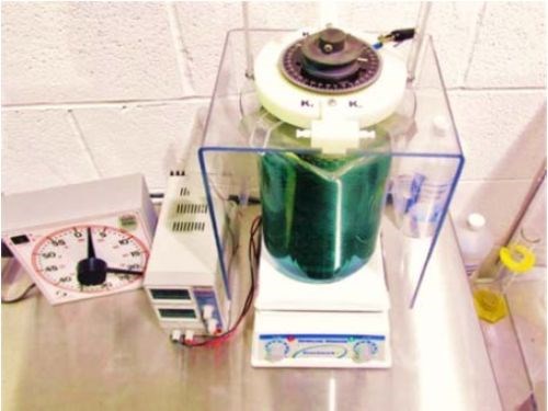
Figure 4 - Typical Test set-up.
B. Plating procedure:
1. Plate each spiral at 2.90 A, 30 A/ft2, for 21 min at 140 ± 1°F for a target deposit thickness of 500 µ-in.
C. Spiral preparation:
1. Clean a spiral as the cathode in an alkaline steel electrocleaner at 5 A for 30 sec, then water rinse.
2. Nickel strike the spiral at 5 A for 2 min, then water rinse and dry.
3. Record the weight of the spiral in grams.
D. Spiral calibration:
1. Calibrate the spiral according to the procedure recommended by the supplier.
2. Determine and record the Kc and Kt degrees.
E. Nickel plate the spirals.
1. Plate the spirals at 2.90 A for 21 min.
2. Tap the top of the contractometer lightly, then read and record the degrees deflection at the arrow point.
F. Calculate and record the average deposit thickness in inches:
1. Formula to calculate deposit thickness follows:
where
T = Deposit thickness (in.)
W = Grams of nickel and
D = Density of nickel = 8.90 g/cm3.
2. For spirals plated on the new design contractometer, the spiral plated surface area is precisely 13.57 in.2 and the following shortened formula applies:
3. For spirals plated on existing contractometers, the spiral must be tightly wrapped around a half-inch diameter rod. The plated length must then be estimated and the diameter (d) and plated length (h) values are used to calculate the plated surface area as follows:
Surface Area = πdh = in.2
G. Calculate deposit stress in PSI:
where
D = Degrees caused by the deposit,
w = Degrees Kt from the spiral calibration,
d = Deposit thickness (in.),
Eo = Modulus of elasticity of the deposit = 30,000,050 for pure nickel, and
t = Substrate thickness (in.) = 0.010 in.
H. Results:
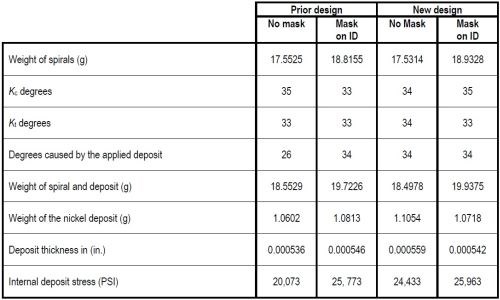
Note: It was observed that deposits on the interior of unmasked spirals were much thicker when plated on a contractometer featuring the prior design. The targeted average test deposit thickness was 500 µ-in., (0.000500 in.). The error for prior versus new between masking and not masking the interior is 24.64% versus 6.26%.
Formulas to calculate deposit stress
Formula for the deposit stress analyzer bent strip method
where
S = Deposit stress (PSI),
K = Test strip calibration constant supplied by the manufacturer,
M = Correction for modulus of elasticity differences between the deposit
and the substrate: M = EDeposit / ESubstrate, and for a nickel deposit over
a copper-iron test strip, M = 206,900 / 120,690 = 1.714,
T = Average deposit thickness (in.) and
U = Total number of increments spread between the test strip leg tips.
Note: Reference Table 1 for the M values for different base and deposit materials and Table 2 for the correction of stress values using the M factor. The tables are located at the end of this paper.
Formulas for Bent Strip with one end stationary (Reference Fig. 5.)
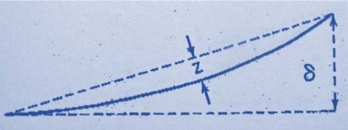
Figure 5 - Bent strip stress curve.
For the comparison of equations that follow to calculate the internal deposit stress of applied metallic coatings over various substrate materials, the value of U = 8.5 units = 0.780 in. will consistently be used as a basis. It will be noted that the calculated internal deposit stress values vary from equation to equation, particularly where the equation fails to address modulus of elasticity differences between the substrate and the deposit.
Relationship between δ and Z
Example: For a given test strip, U = 8.5 units = 0.780 in. and δ = U in inches × 25.385 mm/in. / 2, so in this case δ = 9.90 mm.
δ = 4Z
Z = δ / 4
L = 76.155 mm
Using δ = 9.900 mm, Z = 9.90 mm / 4 = 2.475 mm
R = radius of curvature = =
= 303.34 mm
L = test strip plated length = 76.2 mm
Note: These formulas only work for bent strip applications and are not applicable for the spiral contractometer method.
The Stoney formula
The Stoney formula is typically used to determine deposit stress. However, frequently it is used without consideration for differences in modulus of elasticity values that exist between metallic substrates and the metallic coatings that are applied to them by either electrolytic or chemical reduction processes.
The Stoney formula is not modified to compensate for modulus of elasticity differences between the base metal and the deposit. Example: For a Cu-Fe alloy test strip, U = 8.5 units = 0.780 in. and δ = U in inches × 25.385 mm/in. / 2 = 9.90 mm.
= 91.137 MPa = 13,214.9 PSI. This is an incorrect value.
It is necessary to use a modified Stoney formula with a modulus of elasticity correction where, for copper-iron alloy test strips receiving a deposit of nickel:
M = EDeposit / ESubstrate = 1.714.
where
L = test strip plating length = 76.2mm
M = 206900 / 120690 = 1.714
T = Stock thickness = 0.05077 mm and
t = Deposit thickness = 0.000075 µ-in. = 0.001904 mm
= 156.30 MPa = 22,649 PSI. This is the correct value.
Other relevant formulas
In ASTM Standard B636-84 (2010), a formula is proposed for the correction of the stress value obtained by factoring in the modulus of elasticity difference between the deposit and the substrate for spirals plated on a spiral contractometer.
where
Sr = the truer stress (MPa),
S = the stress value without the modulus of elasticity difference correction (MPa),
EDeposit = the deposit modulus of elasticity,
ESubstrate = the substrate modulus of elasticity,
t = the helix strip thickness (m),
Τ = the helix deposit thickness (m),
W = mass of deposit (kg),
d = density of deposit (kg/m3) and
A = plated area (m2).
Below are other formulas that may be useful for deposit stress calculations. Note that these formulas apply for bent strip applications but do not apply for spiral contractometer applications.
1. Barklie and Davies formula:
2. Heussner, Balden and Morse formula:
3. Brenner and Senderoff formula:
β = EDeposit / ESubstrate = 1.714
σ = 95.538 MPa = 13,853 PSI. This is an incorrect value.
Note: These formulas do not correct for large differences in modulus of elasticity values. The uncorrected Stoney result was 13,215 PSI and the Brenner and Senderoff result was 13,853 PSI.
Useful modified formulas are proposed by the author for correct determinations of internal deposit stress in applied metallic coatings where there is a significant difference in the modulus of elasticity values between the deposit and the substrate materials. To be correct, the Brenner and Senderoff formula requires modification as follows:
β = EDeposit / ESubstrate = 1.714
σ = 156.11 MPa = 22,636 PSI. This is the correct value.
Note: The corrected Stoney formula result above was 22,649 PSI.
Example for electroless nickel applications
Given that E = 55,000,000, this value divided by 145 = 379,310 MPa, the modulus of elasticity for the plated alloy deposit, EDeposit. In the Deposit Stress Analyzer formula, S = UKM divided by 3T. M = the modulus of elasticity of the deposit, EDeposit, divided by the modulus of elasticity of the substrate, ESubstrate. Thus, M = 379,310 divided by 206,900, the modulus of elasticity of the nickel test strip. If pure nickel is plated over a pure nickel test strip, M would equal 1.0. In the case of nickel-phosphorus alloy, however, M becomes 1.833 and the actual internal stress of the deposit is 1.833 times greater than that of a pure nickel deposit applied under similar conditions.
Frequently, the increase that the modulus of elasticity effects on the internal deposit stress of applied coatings is not recognized. Numerous formulas for calculating the internal deposit stress of metallic deposits do not include a correction for the difference of the modulus of elasticity between the deposit and the substrate material. In such cases, the calculated result can be far from the true value. One of the most frequent errors occurs when electroless nickel alloy deposits are calculated using the modulus of elasticity of pure nickel rather than the actual value characteristic of the alloy. Tables 1 and 2 are extremely helpful for evaluating the internal stress in deposited coatings other than nickel.
In regard to testing the internal deposit stress in applied metallic coatings, it is imperative that the difference in the modulus of elasticity values between the deposit and the substrate be part of the calculation equations. The fact remains that this omission is far too common throughout the world, particularly when testing stressed electroless nickel alloy deposits where the modulus of elasticity of pure nickel is frequently used in the equation in error. This mistake is serious because it yields a deposit stress value far less than the actual value and certifications can be false.
Table 1 - Modulus of elasticity values for deposit stress determinations.
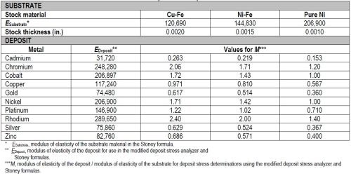
Table 2 - Modulus of elasticity for nickel-phosphorus and nickel-boron alloy deposits.

About the author

Frank Leaman received a Bachelor of Arts Degree in Chemistry from Eastern Mennonite University, Harrisonburg, Virginia. He completed graduate studies at Franklin and Marshall College, Lancaster, Pennsylvania. While working as a Chemist at Dentsply International, York, PA, Frank received a patent for the world’s first electroless platinum plating process. Later, he obtained several additional patents including the platinum coating of anodes having a polysulfone core. While employed by AMP, Inc. in Harrisburg, PA, Frank was responsible for the plating requirements of the Connector and Components Group. During this time, he received numerous cost reduction awards related to selective gold plating. He also conducted research on pulse plating of nickel, gold and palladium, and co-authored with Dr. Jean Claude Puippe, the world’s first textbook on pulse plating, Theory and Practice of Pulse Plating. In 1981, Frank became the owner and President of Electrochemical Company, Inc., a plating job shop that applied metallic coatings by electrolytic and electroless means to comply with specifications for military and aerospace applications. The company also specialized in gold and silver decorative plating. In 1992, Frank established Specialty Testing and Development Company, Inc. As CEO, he provides technical assistance and leads the firm in research and product development.
Related Content
Practical Observations in Surface Chemistry and Boundary Layer Control to Enable Scalable Electrochemical Operation - The 57th William Blum Lecture
This paper is based on the 57th William Blum Memorial Lecture at SUR/FIN 2023, in Cleveland, Ohio on June 8, 2023, by Dr. Tim Hall, recipient of the 2023 NASF Scientific Achievement Award. It focuses on the practical effects of controlling the boundary and surface chemistry on a wide range of electrochemical applications. After a brief introduction to the concept and principles of surface and boundary layer properties during electrochemical processes, the use of this approach in controlling various physical properties during electroplating and electrochemical finishing is discussed, including controlling coating stress and metal composition, as well as enabling simple water-based electrolytes to polish passive or complex materials.
Read MoreSUR/FIN 2023 Registration Is Now Open
The National Association for Surface Finishing SUR/FIN 2023 surface finishing industry trade show will take place June 6-8, 2023 in Cleveland, Ohio.
Read MoreNASF/AESF Foundation Research Project #121: Development of a Sustainability Metrics System and a Technical Solution Method for Sustainable Metal Finishing - 15th Quarterly Report
This NASF-AESF Foundation research project report covers the twelfth quarter of project work (October-December 2023) at Wayne State University in Detroit. In this period, our main effort focused on the development of a set of Digital Twins (DTs) using the Physics-Informed Neural Network (PINN) technology with application on parts rinsing simulation.
Read MoreCalculating Applied Media Force During Vibratory Finishing
What appear to be identically set-up vibratory bowls will finish identical loads of parts in varying time cycles. This paper offers a new technique to better predict what the operator will produce, by measuring the force applied to the parts. It is the efficiency of that force which controls the efficiency and speed of the refinement cycle.
Read MoreRead Next
Episode 45: An Interview with Chandler Mancuso, MacDermid Envio Solutions
Chandler Mancuso, technical director with MacDermid Envio discusses updating your wastewater treatment system and implementing materials recycling solutions to increase efficiencies, control costs and reduce environmental impact.
Read MoreA ‘Clean’ Agenda Offers Unique Presentations in Chicago
The 2024 Parts Cleaning Conference, co-located with the International Manufacturing Technology Show, includes presentations by several speakers who are new to the conference and topics that have not been covered in past editions of this event.
Read MoreEducation Bringing Cleaning to Machining
Debuting new speakers and cleaning technology content during this half-day workshop co-located with IMTS 2024.
Read More








.jpg;maxWidth=300;quality=90)


