In the metal finishing industry, the thickness of a coating can dictate the functionality, appearance and cost of a final product. Coating thicknesses are typically found in the range from 0.1 to 85+ microns, depending on the application, and it is imperative that the thickness of coatings are monitored and controlled. Proper coating thickness is required to ensure consistent part performance and appearance.
Why plating thickness is important

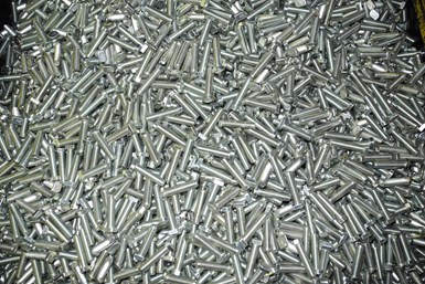
Correct coating thickness for screws is essential for thread ability and tensile strength. Photo credit: Dynamix Inc.
Plating thickness is crucial for functional coatings since the thickness of the coating is proportional to its durability. For example, to improve corrosion resistance, zinc coatings are commonly employed over steel. Zinc undergoes galvanic corrosion when in electrical contact with steel, meaning it is more electrochemically active and corrodes preferentially when compared to steel. Products designed to work in corrosive environments will require a minimum thickness of zinc to guarantee the lifetime of the final product. Similarly, copper deposits used for conductivity applications will have strict thickness requirements to make certain that the deposit has the correct current-carrying capacity.
In decorative applications, plating thickness is equally important, as it often relates to appearance. For example, decorative chrome deposits should not be in excess of one micron or else the deposit may lose its lustrous appearance. In decorative gold plating, a minimum thickness should be achieved with little excess to ensure that the expensive, precious metal is not over-consumed. Attaining and controlling the proper coating thickness is crucial in both functional and decorative applications.
Causes of improper thickness
When insufficient plate is observed, often the electroplating bath has a source of inefficiency. There are numerous examples of an inefficiency that causes insufficient plating thickness in electroplating processes. For example, in chrome plating, poor chromium coverage can be a result of low chromium concentration or a low chromium to catalyst ratio. A lower chromium content reduces the ability of the metal to deposit evenly across the substrate and can result in partial coverage and premature part failure. Partial coverage can also be observed in electroless nickel deposits when the bath becomes over-stabilized. Stabilizers present in electroless nickel baths help keep nickel in solution. When present in excess, however, stabilizers prevent the nickel from plating out onto the substrate and can result in poor nickel coverage. Contaminants can also affect the throw of an electroplating solution. The throw of a solution is the ability to plate in recesses or low current density (LCD) areas. For example, in chloride zinc electroplating, contamination from metals like copper, lead and cadmium can result in poor LCD plating and lead to pinpoint rusting in those areas.
In contrast with insufficient plating thickness, excessive plating thickness is often associated with HCD areas on a part. Since different parts have varying geometries and different degrees of HCD, buildup in these areas is a constant battle amongst electroplaters. Many chemical suppliers, like Dynamix, provide proprietary chemical additives to help level deposits by preventing buildup. Often called “carriers” or “levelers,” these additives interact with HCD areas and provide a consistent plating environment across the entirety of the substrate to provide a uniform and leveled deposit. For parts with very unique geometries, consider using conforming anodes to compensate for areas of LCD/HCD to ensure no buildup is found in HCD areas.
Common problems caused by improper coating thickness
Without controlling the thickness of coatings, applicators risk achieving an insufficient or excessive coating thickness – both of which can be problematic. In the case of an insufficient plating thickness, common issues include partial coverage, pinpoint rusting and brittle deposits.
Partial coverage is identified as when the substrate or subsequent coatings have bare spots after plating. This defect can be visible, which detracts from the appearance of the product and can also lead to premature part failure. Voids in the coating can introduce corrosion sites on the substrate or cause damages/discoloration from UV degradation, all of which compromise the integrity of the product.
Pinpoint corrosion is observed when an insufficient coating thickness does not provide enough cathodic protection over the base metal. As a result, the coating will fail to provide enough corrosion protection across the entirety of the part and rust spots will develop. Similar to partial coverage, this issue threatens the appearance and functionality of the part.
Insufficient coating thicknesses can result in brittle deposits. Plated deposits have a tendency to imitate the crystal structure of the underlying metal substrate during the initial atomic layers. This phenomenon is exemplified in decorative chrome applications, where chromium can achieve its lustrous appearance from the underlying bright nickel deposit. While this feature has aesthetically pleasing results, the assumed crystal structure also imposes stress and brittleness in the deposit. Especially in functional coatings like sulphamate nickel, the brittleness achieved by insufficient plating can be disastrous.
While insufficient plating thickness can cause numerous issues, serious problems can also be caused by excessive coating thickness. Excessive coating thickness is commonly found on high current density (HCD) areas on a part. HCD areas are often associated with edges or sharp points on parts that are close to the anode and, as a result, receive the highest current density. Deposits tend to buildup in HCD areas which can cause dimensional issues, especially for parts with tighter dimensional tolerances. For example, parts used for fittings or threaded parts, like screws, will have tight thickness requirements to ensure the coating thickness does not hinder the functionality of the part.

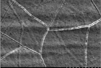
Cracked chrome deposit. Photo credit: Dynamix Inc.
Excessive plating thickness can also result in brittle deposits. Excessive buildup introduces a great deal of internal stress within the metal deposit, which can cause the deposit to crack, leading to structural and visible damage. Finally, unnecessary buildup is costly as it wastes resources and time to achieve.
Measuring and monitoring coating thickness
To avoid issues caused by improper coating thicknesses, it is important to measure and monitor coating thicknesses of both decorative and functional coatings.

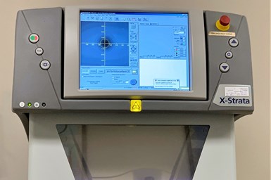
The X-ray fluorescence spectrometer at Dynamix. Photo: Dynamix Inc.
One instrument commonly used for this function is the X-ray fluorescence spectrometer (XRF). This non-destructive instrument uses X-rays to probe the thickness of different metallic coatings. The XRF operates by focusing an X-ray on the sample, which excites the metal coating, causing it to emit a unique, secondary X-ray. The XRF measures the secondary X-ray produced from the coating and, depending on the energy and intensity of the radiation, the instrument can calculate both the composition and thickness of the coating with extreme accuracy. Using different laboratory standards, an XRF can measure the thickness and composition of any metallic coating over any substrate. While the laboratory-grade XRF at Dynamix is very expensive and requires training and regular maintenance, handheld XRFs (HXRF) are becoming widely available. HXRFs operate under the same principle as laboratory XRFs and provide accurate readings while being more affordable and easier to use. While the XRF does provide reliable readings, it is difficult to measure layers that are composed of numerous elements, like metal oxide layers, or multilayered deposits consisting of the same element, like a semi-bright and bright nickel multilayer. As such, other measurement techniques are employed.
One technique employed to measure metal-oxide coatings uses eddy current. An eddy current thickness gauge uses a nondestructive method to measure nonconductive surfaces over nonferrous substrates using a magnetic field. The gauge emits a magnetic field which penetrates the nonconductive layer and induces an electrical current in the substrate called an eddy current. The thickness gauge measures eddy current strength and the respective magnetic field produced and then calculates the thickness of the nonconductive coating. This test is often employed to measure the thickness of anodized aluminum and can also be used to measure phosphate coatings and paint thicknesses. Eddy current thickness gauges are inexpensive and follow a straightforward operating procedure. However, eddy current gauges can struggle to report precise measurements when the base substrate surface is rough, like in zinc die castings. The eddy current induced on rough surfaces produces varying signals, which limits the ability of the gauge to accurately report thicknesses.
Another measurement method regularly used in the Dynamix lab is the simultaneous thickness and electrochemical potential (STEP) test. This is a destructive method usually employed to measure multiplex nickel products. This is a coulometric test, meaning the test measures anodic dissolution under a constant current. Based on differing sulfur content in different nickel layers (i.e. semi-bright vs. bright), the time it takes to dissolve each layer is related to the thickness of that layer. A difference in voltage indicates a change in sulfur content and thus can be used to differentiate between two different nickel layers. The STEP test can accurately measure different nickel thicknesses while also measuring the electrochemical potential between the two layers, which is a crucial requirement for a lot of automotive applications. The STEP test can be used to measure the thickness of numerous electroplated coatings, both single or multilayer, but, again, is most commonly used for nickel coatings. While this test is effective, it is a destructive test, so samples used for this test are scrapped after testing.
Related Content
SUR/FIN 2023: Capsules from the Technical Sessions I: Emerging Technologies
SUR/FIN 2023 in Cleveland this past June was a resounding success. Due to the efforts of the Technical Activities Committee, ably led by Bill Nebiolo this year, an outstanding program of technical presentations was offered. What follows are summaries of selected presentations from the Emerging Technologies sessions. Additional coverage will be provided in this space in the coming months. The full report can be accessed and printed at short.pfonline.com/NASF23Aug1.
Read MorePowder Coating Overcomes Post Forming
Six Sigma methodology, open communication, and collaboration produce results for leading boat manufacturer.
Read More5 Things to Know About XRF Calibration
The proactive approach of validating measurement performance and calibrating only as often as necessary improves quality, consistency and reduces costs.
Read MoreAESF Heritage: The 2002 Hydrogen Embrittlement Seminar No. 4: Hydrogen Embrittlement – A Personal View
This is last of four papers presented during AESF Week 2002 at the Rosen Center in Orlando, Florida on January 30, 2002, as part of the Hydrogen Embrittlement Seminar. This paper presents a comprehensive overview of the research into hydrogen embrittlement at the turn of the century. The full paper on this work can be accessed and printed at short.pfonline.com/NASF24Sep4.
Read MoreRead Next
Delivering Increased Benefits to Greenhouse Films
Baystar's Borstar technology is helping customers deliver better, more reliable production methods to greenhouse agriculture.
Read MoreEducation Bringing Cleaning to Machining
Debuting new speakers and cleaning technology content during this half-day workshop co-located with IMTS 2024.
Read MoreEpisode 45: An Interview with Chandler Mancuso, MacDermid Envio Solutions
Chandler Mancuso, technical director with MacDermid Envio discusses updating your wastewater treatment system and implementing materials recycling solutions to increase efficiencies, control costs and reduce environmental impact.
Read More


.jpg;maxWidth=300;quality=90)


