Self-Induced Repair of Printed Circuit Boards
This is a re-publication of the 1992 AESF Gold Medal Award paper for best paper published in Plating & Surface Finishing in 1991. It introduces a then-new technique for repairing near-opens (constrictions) in the wiring on printed circuit boards has been developed.
Editor's Note: Originally published as C.J. Chen, et al., Plating and Surface Finishing, 78 (6), 45-49 (1991), this paper received the AESF Gold Medal Award for Best Paper published in Plating & Surface Finishing for the year 1991. A printable version of this paper can be accessed HERE.
ABSTRACT: A new technique for repairing near-opens (constrictions) in the wiring on printed circuit boards has been developed. It is based on a local copper plating process induced by the Joule heat generated at the defect site. It is self-locating, that is, it does not require the actual location of the defect in the line (circuit trace) to be identified. It is self-terminating; the process stops by itself when the defect is cured. By adding a simple laser seeding step, circuit opens can be repaired, and new interconnections created at will. The repairs and customized interconnections generated by this new technique have the same quality as the original circuit traces.
Printed circuit boards (PCB) fresh from the plating tank or etching tank often have defects. Therefore, testing and repairing are among the most essential steps of the manufacturing process. For near-opens, a commonly used method is to apply a high current pulse to each trace to blow them up, then treat them as circuit opens. For circuit opens, the commonly used method is to solder or braze them with small pieces of copper wire or ribbon. As the density of circuits becomes higher and higher, this method is becoming increasingly difficult to practice.
In this article, a new process called self-induced repair (SIR) is described. The basic idea is to utilize the Joule heat generated at the constriction site to induce local copper plating, thus, to convert the constriction to normal thickness.1 To repair circuit opens, or to make new connections, a prior laser-seeding step is executed to generate a conducting film along the desired path. No matter how poor the initial conductance, the SIR process will restore it to normal.2
Figure 1 shows the schematic of SIR. A PCB is submerged in a plating solution, which typically contains 1M CuSO4 and 0.25M H2SO4. An alternating current is passed through the defective trace. Because the constriction site has a higher electrical resistance and a lower heat conductance than the normal part of the trace, it becomes warmer, as shown in Fig. 2. The thermobattery effect causes the warm part to become cathodic and the cool part anodic. Positive copper ions are attracted to the constriction. When the defect site is built up sufficiently for a decrease in Joule heat, even with a reasonably high current, the local plating process terminates automatically.
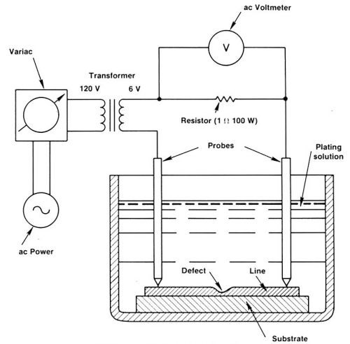
Figure 1 - A simple apparatus for demonstrating self-induced repair.
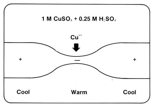
Figure 2 - The principle of self-induced repair: local electroplating induced by Joule heat at a constriction.
Thermobattery effect is simply a term to describe the temperature dependence of the equilibrium electrode potential.3,4 Figure 3 shows a simple experiment for demonstrating this effect. A glass U-tube, with two identical copper electrodes, is filled with plating solution. By heating one of the two water jackets, using the heating coil, the DC millivoltmeter will show a non-zero reading. By letting it cool down naturally, complete curves (equilibrium cell potential vs. temperature difference) can be recorded.* Typical curves are shown in Fig. 4. Experiments show that the slope of the curves (the temperature coefficient of the equilibrium electrode potential) is independent of the concentration of H2SO4, but depends sharply on the concentration of CuSO4, which is expected from the Nernst equation.1 With a temperature rise of 50°C, a cell voltage of 30 mV can be generated. Experiments also show that the warm electrode is always positive. If the two electrodes are connected with a wire, copper ions will migrate to the warm electrode. The plating rate induced by such a thermobattery effect is typically a few microns per minute. Therefore, a constriction can be built up in just a few minutes.
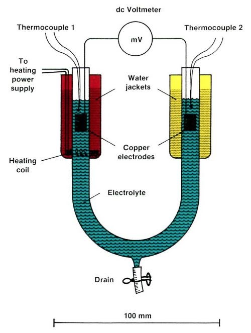
Figure 3 - An electrochemical cell for measuring the temperature dependence of the equilibrium electrode potential (the thermobattery effect).
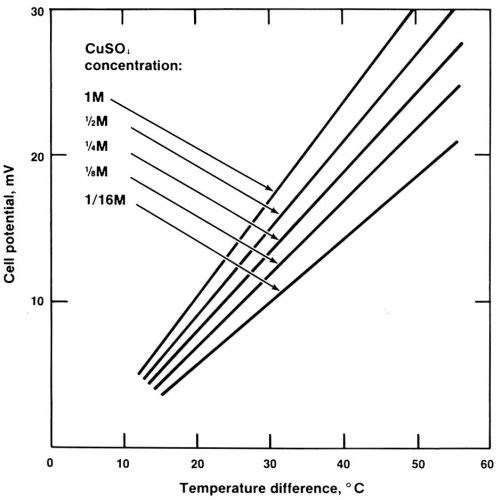
Figure 4 - Dependence of cell potential on temperature difference of the electrodes.
To execute the SIR process properly, alternating current must be used. If DC is used, the two sides of the trace will have a voltage difference. Consequently, copper will deposit on one side and dissolve on the other, and the trace will become asymmetric. Pure alternating current generates plating only at the defect site. Different kinds of AC power sources have been tested, with the result that within the audio range, i.e., up to a few kHz, the process is independent of both frequency and waveform. Thus, the simplest way to do the experiment is to use commercial 60-Hz power, as shown in Fig. 1. A variac and a transformer are used to reduce the line voltage to a few volts. Current is fed into the defective circuit trace through a one-ohm power resistor and a pair of copper probes. The current is monitored with a digital voltmeter across the power resistor. Thus, the one-ohm resistor is used to stabilize the current as well as monitor it. Of course, for production lines, a computer-driven AC source is preferred.
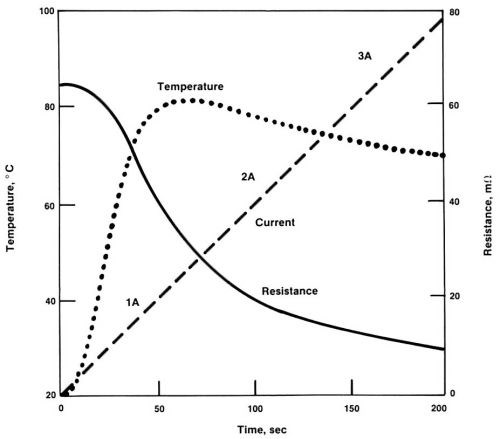
Figure 5 - The current ramping process for self-induced repair.
To avoid overheating, as well as underheating, the current must be carefully controlled. Though this appeared difficult, it was found that by ramping the AC slowly from zero to the rated current of the normal trace, the process becomes self-regulating,1 as shown in Fig. 5. At first, there is no action. When the current reaches a point where the temperature at the defect induces substantial plating, the defect becomes partially cured. As a result, the trace can tolerate a higher current. Finally, the current reaches the rated value (the maximum the trace can tolerate). If part of the trace is still too narrow, copper will deposit at this spot to make it thicker and broader. The repairing current is then maintained at the maximum value for a couple of minutes. The local plating process stops automatically when no part of the trace is overheated under the rated current.
If there are multiple constrictions in a trace, they may be repaired in a single operation. By ramping AC into the trace, the most severe defect gets heated first, and so, plated first. When it is comparable to the next most severe defect, both defects are plated at the same rate. The process continues until the entire trace becomes more or less uniform.
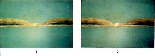
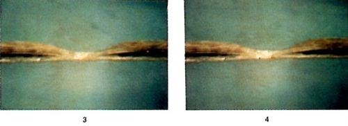
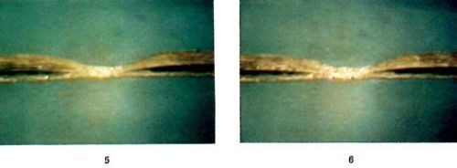
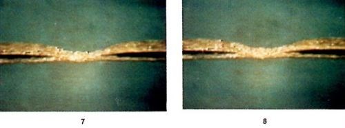
Figure 6 - Photographic sequence showing the evolution of a defect under self-induced repair, reproduced from a video tape. Time interval between frames: 10 seconds.
Figure 6 shows a sequence of photographs of a defect undergoing self-induced repair, reproduced from a video tape. The samples are small pieces of epoxy-glass PCB with a copper trace about 40 μm thick and 150 μm wide. The constrictions in the traces were made through local etching with ferric chloride solution to desirable dimensions. The electrolyte contains 1M CuSO4 and 0.25M H2SO4. The 60-Hz AC was ramped from 1A to 4A at a rate of 2A per minute. The sample is tilted by 45° with respect to the optical axis of the video-camera lens to obtain good perspective. The time interval between consecutive frames in Fig. 6 is 10 seconds. As shown, the deposition process begins at a small hot spot at the center of the constriction. The copper deposition becomes thicker and larger with time. Through the microscope, it is observed that many shiny spots are moving around in the region of copper deposition. In fact, as shown later in the scanning electron microscope (SEM) micrographs, the shiny spots are facets of tiny copper crystals changing size and orientation during the deposition process. Later, copper deposition spreads to both sides of the constriction.
Figure 7 is an SEM micrograph of the surface at the center of the SIR copper deposition. As shown, the deposited copper appears crystalline and continuous, with grain size of 1 to 5 μm. It has the dense texture typical of plated copper.
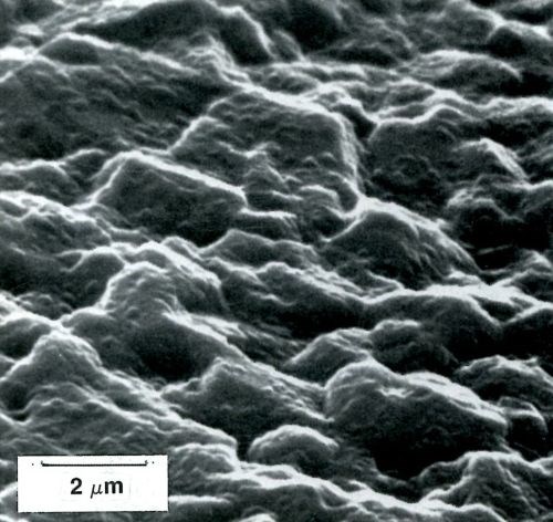
Figure 7 - Scanning electron micrograph of copper deposition at the center of a defect, generated by self-induced repair.
To repair circuit opens or make new interconnections, a seeding step is needed. Although there are many different ways to make seeded interconnections, it was found that the laser-induced pyrolytic decomposition process from a solid-film of an organometallic compound is convenient and inexpensive, as shown in Fig. 8. First, an organometallic film is applied on the substrate. Second, a focused laser beam is scanned along the path to be seeded. A metal film is then generated along the desired path. Third, the residual organometallic film is washed off with a solvent, e.g., the same solvent used for spraying it.
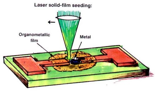
Figure 8 - Laser seeding for repair opens and making customized interconnections using self-induced repair.
A proven formula for the spraying fluid is one gram of palladium acetate (PdAc) dissolved in a mixture of 8 mL of chloroform and 2 mL of methyl alcohol.5 By using a commercial air brush, for example, a uniform brown film of PdAc can be formed on the substrate. An argon ion laser, with an output up to 100 mW at 514 nm or 488 nm or both, is suitable for seeding.
The laser seeding apparatus is shown in Fig. 9. All the operations are conducted in air. Thus, it is much simpler than laser chemical vapor deposition, which needs a sophisticated vacuum chamber and gas handling system.6 In addition, because the function of seeding is to provide an initial conducting path, the electrical quality of seeded connections is not critical. Therefore, the process window is very wide. The following results are from a systematic study of operational conditions:
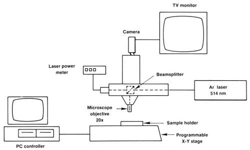
Figure 9 - Apparatus for laser seeding.
Figure 10 shows the resistance of the seeded palladium trace per unit length as a function of laser power and PdAc film thickness. Actually, as long as the PdAc film along the desired path is fully decomposed, the seeding is almost always effective.
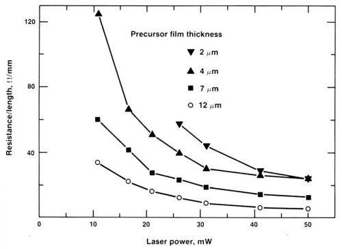
Figure 10 - Dependence of the resistance of the seeded connections on laser power.
Figure 11 shows the width of the Pd trace as a function of laser power and PdAc thickness. As shown, the major factor in width control is laser power.
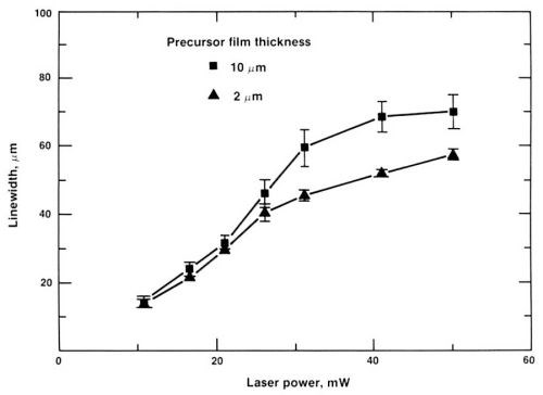
Figure 11 - Dependence of the trace width of the seeded interconnection on laser power.
Figure 12 shows the effect of scan velocity on trace width. As shown, trace width remains constant over two orders of magnitude of scan velocity. Again, a very wide process window was observed.
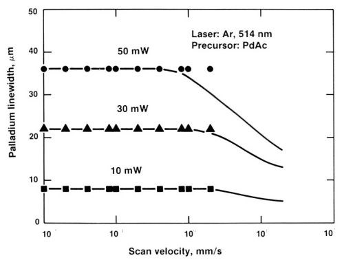
Figure 12 - Effect of scan speed on trace width, showing that trace width is almost independent of scan speed.
A typical customized connection made through this two-step process is shown in Fig. 13: part (a) shows two traces to be connected; (b) a palladium pattern generated by spraying a thin film of PdAc, followed by a programmed laser scan. The width of the Pd trace is 14 μm; (c) the copper trace after SIR. As can be seen from the photograph, the deposited copper is uniform and continuous. Also, the shiny copper deposition extends to the ends of the original trace, making the entire pattern an integrated piece of solid copper.
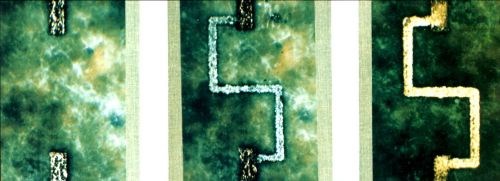
Figure 13 - Example of customized interconnections made with laser seeding and self-induced repair: (1) two leads with a spacing of 0.2 mm; (2) after seeding with palladium, resistance is about 100 ohms; (3) after self-induced repair, resistance is about 50 mohms.
Figure 14 shows a typical cross section of the traces generated by this process. As shown, the cross-sectional area of copper can be orders of magnitude greater than that of the palladium seed material.
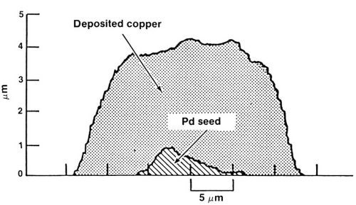
Figure 14 - A typical cross section of customized interconnections made through laser seeding and self-induced repair.
Summary
A self-inducing method for repairing near opens in printed circuit boards has been described. This process is self-locating, self-limiting, and provides high-quality copper deposition. By using a prior laser-seeding step, this method can be used for repairing circuit opens as well as creating customized interconnections.
Acknowledgments
The authors wish to thank Joseph Demuth, Robert von Gutfeld, Lubomyr Romankiw, David Rath and Madhav Datta for helpful discussions as well as Alfred Sturm, Carmelo Aliotta, and Donald Vigliotti for technical assistance.
References (#5 updated)
1. C.J. Chen, Appl. Phys. Lett., 56, 2411 (1990).
2. A. Gupta and C.J. Chen, Appl. Phys. Lett., 56, 2516 (1990).
3. K.J. Vetter, Electrochemical Kinetics, Academic Press, New York, NY, 1967; pp. 15-16.; A.J. Bard and L.R. Faulkner, Electrochemical Methods, Fundamentals and Applications, John Wiley & Sons, New York, NY, 1980; p. 49.
4. J.Cl. Puippe, R.E. Acosta and R.J. von Gutfeld, J. Electrochem. Soc., 128, 2539 (1981); R.J. von Gutfeld, R.E. Acosta and L.T. Romankiw, IBM J. Res. Develop., 26, 136 (1982).
5. J.P. Partridge, B. Hussey, C.J. Chen, and A. Gupta, IEEE Trans. on Components, Hybrids and Manuf. Technol., 15, 252-257 (1992).
6. Laser Microfabrication: Thin Film Processes and Lithography, D.J. Ehrlich and J. Tsao, Eds. Academic Press, Boston, MA, 1989.
About the Authors
Dr. C. Julian Chen is a research staff member at the IBM Watson Research Center, P.O. Box 218, Yorktown Heights, NY 10598. Known in China as an inventor and translator of technical treatises, he was one of the first Chinese scientists awarded a fellowship from a major U.S. university (in 1979). Dr. Chen received the equivalent of a M.A. in physics from Beijing University and his Ph.D. in physics from Columbia University. He worked on laser materials processing at Columbia, prior to joining IBM, where his research interests include the self-induced repair process he invented, and scanning tunneling microscopy.
Dr. Julian Partridge is employed by the IBM Systems Technology Division, Austin, TX. He obtained a B.S. in materials science from the University of Bath, U.K., and a M.S. in metallurgy from Cranfield Institute of Technology, U.K. He received a Ph.D. in metallurgy from the Institute of Materials Science, University of Connecticut, where he studied laser materials processing.
Brian Hussey is a senior associate engineer in physical sciences at the IBM Watson Research Center. He received an A.B. degree in physics from Dartmouth College and was employed by Philips Laboratories in the areas of laser-stimulated luminescence of II-VI compounds and x-ray phosphors. His current technical interests include superconducting thin film growth by laser ablation, laser applications in deposition and etching and process control electronics.
Dr. Arunava Gupta attended the Indian Institute of Technology, Kanpur, where he received his M.S. in chemistry. He came to the U.S. and obtained a M. Phil., from Columbia University and a Ph.D. in chemical physics from Stanford. As a research staff member at the IBM Watson Research Center, he started a group working on laser applications and has worked on various photothermal and photochemical laser techniques for processing and patterning of materials. Since 1987, he has been primarily involved in growth and characterization of high-temperature superconducting oxide thin films.
Footnote:
* When the hot end is cooled to room temperature, the voltage may differ from zero because the surfaces of the electrodes have been changed during heating. By repeated cycling, however, the slope is always reproducible. Therefore, the measurement is still meaningful.
Related Content
Products Finishing Reveals 2023 Qualifying Top Shops
Each year PF conducts its Top Shops Benchmarking Survey, offering shops a tool to better understand their overall performance in the industry. The program also recognizes shops that meet a set of criteria to qualify as Top Shops.
Read MoreTroubleshooting Alkaline Zinc
One of the most common problems that can arise when plating with alkaline zinc is an imbalance of brightener in the solution. In this helpful Ask the Expert article, Chad Murphy of Columbia Chemical discusses how different zinc metal concentrations and brightener concentrations can impact efficiency.
Read MoreAn Overview of Electroless Nickel Plating
By definition, electroless plating is metal deposition by a controlled chemical reaction.
Read MoreTrivalent Chrome Overview
As the finishing industry begins to move away from the use of hexavalent chromium to trivalent chromium, what factors should finishers consider as they make new investments? Mark Schario, chief technology officer for Columbia Chemical offers a helpful overview of this complicated topic.
Read MoreRead Next
A ‘Clean’ Agenda Offers Unique Presentations in Chicago
The 2024 Parts Cleaning Conference, co-located with the International Manufacturing Technology Show, includes presentations by several speakers who are new to the conference and topics that have not been covered in past editions of this event.
Read MoreEpisode 45: An Interview with Chandler Mancuso, MacDermid Envio Solutions
Chandler Mancuso, technical director with MacDermid Envio discusses updating your wastewater treatment system and implementing materials recycling solutions to increase efficiencies, control costs and reduce environmental impact.
Read MoreDelivering Increased Benefits to Greenhouse Films
Baystar's Borstar technology is helping customers deliver better, more reliable production methods to greenhouse agriculture.
Read More






.jpg;maxWidth=300;quality=90)
