Simultaneous Thickness and Electrochemical Potential Determination of Individual Layers in Multilayer Nickel Deposits
The 1981 AES Gold Medal Award was given to Ed Harbulak for the Best Paper appearing in Plating and Surface Finishing in 1980. His work involved the development of the well-known STEP test, a method for evaluating the performance of decorative Cu-Ni-Cr, measuring the electrochemical potential of nickel multilayers with a modified version of the venerable Kocour thickness tester.
by
Edward P. Harbulak
Chrysler Corporation
Detroit, Michigan
Editor’s Note: Originally published as E.P. Harbulak, Plating and Surface Finishing, 67 (2), 49-54 (1980), and was awarded the 1981 AES Gold Medal for Best Paper published in Plating and Surface Finishing in 1980. A printable PDF version is available by clicking HERE.
ABSTRACT
The corrosion protection provided by multilayer nickel deposits is related to the electrochemical potential difference between the individual nickel layers. A simple procedure for simultaneously determining the thickness, relative electrochemical potential and polarity of the individual layers of a multilayer nickel deposit is described. A commercially available thickness tester was modified to display results on a chart recorder. Representative results obtained for duplex and triple-layer nickel deposits are presented along with data on defective deposits.
Introduction
Multilayer electrodeposits consisting of sulfur-free semibright nickel, sulfur-containing bright nickel and microdiscontinuous chromium constitute the preferred plating system for severe service applications such as exterior automotive hardware.1 The efficacy of duplex nickel coatings is a function of the electrochemical potential difference between the sulfur-free semibright nickel and the more active sulfur-containing bright nickel.2-4 A sufficient potential difference between the two nickel layers causes the bright layer to corrode preferentially and sacrificially with respect to the semibright nickel. This in turn retards the rate of penetration through the total nickel deposit and gives better (i.e., longer) corrosion protection to the basis metal than a single-layer nickel deposit of equal thickness. A 30.5 μm (1.2 mil) deposit of duplex nickel is superior to 51 μm (2.0 mil) of either semibright or bright nickel present as a single-layer deposit, each with 0.25 μm (0.010 mil) of chromium.5 The inclusion of a thin, very active nickel layer between the semibright and bright nickel layers can provide an additional increase in corrosion protection.6
In order to obtain the best possible corrosion protection from a multilayer nickel microdiscontinuous chromium deposit, certain conditions must be met. An adequate minimum thickness for each of the individual nickel layers as well as the proper thickness ratio of semibright to bright nickel are the most obvious requirements for satisfactory results. Of equal or even more importance, is a sufficient electrochemical potential difference between the various nickel layers together with the proper activity or polarity of the nickel layers. These last two items constitute the basis for the duplex effect. Finally, if a microdiscontinuous chromium deposit is used, it is essential that an adequate crack or pore count be achieved across the entire useful current density range of the plated part.
A variety of satisfactory procedures has been developed for measuring total deposit thickness. However, thickness measurements of the individual layers in a multilayer nickel deposit normally can only be made by sectioning, mounting, metallurgically polishing and etching a sample of deposit. The individual layers are then measured microscopically.7 The Dubpernell Test,8 or a recent modification,9 makes it easy to determine the crack or pore count in the microdiscontinuous chromium layer. Unfortunately, it has been virtually impossible to readily measure the electrochemical potential of the separate nickel layers in a multilayer nickel deposit, especially on a finished part. The individual nickel potentials are ordinarily determined by obtaining a foil or other nickel sample from the specific nickel plating bath used to plate the nickel layer in question, and measuring the open circuit potential.10 After the electrochemical potential is determined for a sample of nickel metal from each of the baths used to plate a multilayer nickel deposit, the potential difference between layers is calculated.
Because of the frequent need to measure the thickness of the individual nickel layers in multilayer nickel deposits, experiments were carried out to determine the feasibility of making the measurements using a coulometric method, with the hope that the time-consuming microscopic procedure could be avoided. During the development of a relatively simple and rapid test, it was found that the test procedure simultaneously permitted the measurement of the electrochemical potential difference between the nickel layers as well as the relative deposit polarities. (Simultaneous Thickness and Electrochemical Potential suggests the acronym "STEP" as a descriptive name for the test.)
Development of procedure and equipment
Thickness testers based on the anodic dissolution of the deposit are essentially cells in which the reaction of interest is at the anode. Knowing the area being deplated, the stripping current and time, plus the electrochemical equivalent weight and density of the metal being stripped, it is possible to calculate the deposit thickness using Faraday's Laws, provided the current efficiency at the anode is known.
If the plated metal being stripped is more easily dissolved in a particular electrolyte than the substrate under the plate, a relatively large voltage change is observed across the deplating cell when stripping is completed. This property was exploited to build a device which amplified the voltage change and actuated a relay which, in turn, stopped an electric timer which had been started at the beginning of the deplating operation.11 With this device, the deplating time and deposit thickness could be measured. A commercial thickness tester* makes use of this principle. This and similar testers will rapidly measure the total deposit thickness of most commonly plated metals with an accuracy of ±10%.12-14
By monitoring the potential changes across a deplating cell and recording the voltage as a function of time on a chart recorder, thicknesses of a sulfamate nickel deposit over a Watts nickel deposit have been measured.15 Because the power supplies used in coulometric stripping devices are designed to provide constant current but variable voltage, small voltage changes produced by differences in the electrochemical activity of the various nickel layers in multilayer deposits can be easily obscured by voltage changes originating in the power supply. Consequently, measuring voltage variations across a deplating cell is not a reliable way of measuring the thickness of individual nickel layers. A device for determining the thickness of tin and tin-iron alloy deposits on ferrous substrates has recorded the potential difference developed between the deposit being stripped and a reference electrode.16 This greatly reduced the problem of voltage variation mentioned above. Although this procedure apparently had not previously been exploited for measuring thickness or potential differences between semibright and bright nickel layers, the author discovered that it could be useful for this purpose.
To make the measurements described in this paper, a regulated, constant-current power supply and a sensitive millivoltmeter and/ or chart recorder are required in addition to a suitable stripping cell. The millivoltmeter and the chart recorder should have an input impedance of at least one megohm to prevent loading of the anode-reference electrode couple. The deplating cell contains the electrolyte, a reference electrode, the cathode, an anode of known area and provision for solution agitation at the anode to prevent concentration polarization. Rather than constructing such a device, it is easier and more convenient to modify the aforementioned, commercially available thickness tester, which is fully transistorized and provides the constant current source, a timer calibrated in deposit thickness units and a deplating cell that meets the above requirements.
Although this tester is designed to automatically turn the current off and stop the thickness counter when the deposit has been stripped to the substrate, it is best to keep the current on after the deposit is stripped in order to prevent premature termination of the test when stripping multilayer deposits with relatively large interlayer potential differences. To defeat the automatic shut-off feature of the device, a toggle switch was wired across the "Start" button and used to start and stop each test (The original "Start" switch may be used in its normal mode when the toggle switch is off.). Figure l shows how the toggle switch was installed.
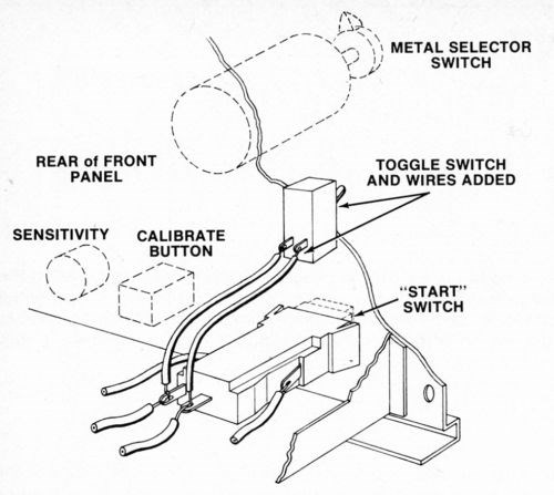
Figure 1 - Location and connection of toggle switch on front panel of thickness tester.
A silver or platinum wire reference electrode was located inside the agitator tube where it made good contact with the electrolyte but was physically out of the way. While a number of satisfactory arrangements are possible, Fig. 2 shows assembly that is sturdy, inexpensive and easily constructed from readily available materials. Figure 3 shows the electrical interconnections between the modified thickness tester and the millivoltmeter and/or chart recorder. For the sake of neatness, the electrical connection between the millivoltmeter/recorder and the anode (deposit being stripped) can be made inside the thickness tester where the red wire with the alligator clip connects to the "Accessory Unit" or "WT" jack. The connection to the reference electrode may also be routed through the thickness tester and both wires may then be connected to a jack mounted on the case of the instrument. However, all connections may be made externally if desired.
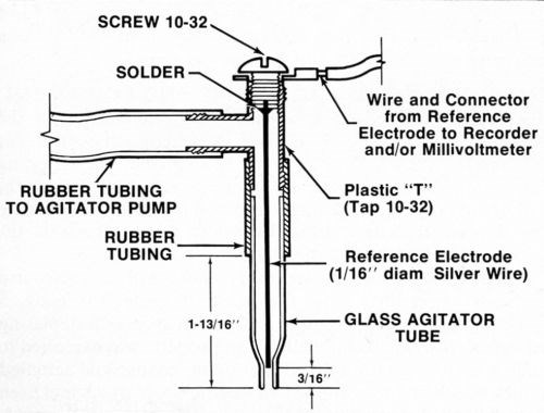
Figure 2 - Modified agitator tube assembly containing reference electrode.
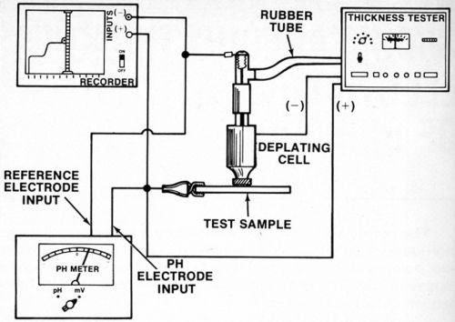
Figure 3 - Electrical connections between recorder, millivoltmeter, reference electrode, test sample (anode) and thickness tester.
Because of the fragile nature of saturated calomel electrodes, space limitations in the stripping cell and maintenance problems, wire reference electrodes are more practical. Silver is perhaps the best choice for the reference electrode, based on effectiveness, availability, ease of maintenance and precedent.16 Although not the normal method for preparing a silver/silver chloride electrode, in the presence of acidic chloride-containing electrolytes, the silver wire reference electrode becomes a satisfactory silver/silver chloride electrode.
Probably the most sensitive and accurate millivoltmeter, with the required high input impedance, is a pH meter. Any pH meter capable of reading ±1100 mV or more should prove satisfactory for making the potential measurements. A vacuum tube voltmeter or one of the new transistorized voltmeters also will give good results if it has a high enough input impedance and a usable low-voltage range.
The potential differences between layers in a multilayer nickel deposit can be measured using only a suitable millivoltmeter, but more definitive results are obtained if the potential variations developed during anodic stripping are recorded with an X-Y or strip chart recorder. The recorder is particularly useful when examining relatively thin nickel layers that are stripped through rather quickly, making it difficult to read the rapidly changing potential values. The permanent record also makes visual evaluation and comparison easier. The recorder should have a chart speed of about 2 cm/min (0.8 in./min) while the input range of the recorder may be between about 40 and 200 mV/cm (100 and 500 mV/in.). If the pH meter used to measure millivolts has recorder output terminals, the recorder input should be connected to the output of the pH meter rather than directly to the anode and reference electrode. A pH meter generally can be expected to have a higher input impedance than a chart recorder and will serve as a good buffer between the recorder and test cell.
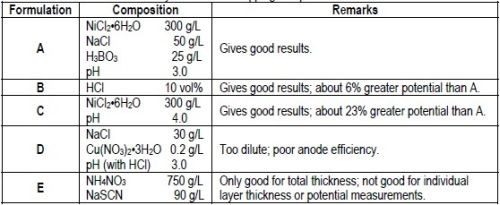
An electrolyte that provides 100% anode efficiency and does not interfere with the test is necessary for stripping the nickel deposit. Although many electrolytes probably would give satisfactory results, Table 1 lists three solution compositions that were useful.
Table 1 - Electrolytes for nickel stripping and potential measurements.
Test procedure
With the equipment set up as described above, a typical procedure for determining the thickness of and potential difference between layers in a multilayer nickel deposit is as follows:
- Turn on the thickness tester, millivoltmeter and recorder and allow several minutes warm-up time.
- Follow the manufacturer's instructions for calibrating and adjusting the instruments being used.
- If chromium is present on the nickel sample, remove it with concentrated hydrochloric acid in the area to be tested. Make sure the area being tested is free of water breaks, dirt, etc.
- Position the cell on the spot to be tested (following manufacturer's instructions).
- Add electrolyte to the cell and position the agitator tube containing the reference electrode.
- Double check all electrical connections. (Don't forget to connect the positive lead to the test part.)
- Use the toggle switch to start the modified thickness tester and simultaneously start the recorder pen or chart.
- While observing the chart recorder to determine which layer of nickel is being stripped, read the millivolt value for that layer from the meter. Alternatively, the millivolt difference between nickel layers may be determined graphically from the chart. When the various nickel layers are stripped, as determined by "steps" in the recorded graph, note the thickness on the instrument thickness "counter."
- When the deposit has been stripped through to the basis metal, turn off the recorder chart drive and stripping current. Occasionally the current will remain on even after the toggle switch is turned off. In that case, press the "stop" button to turn the current off.
Although this procedure is relatively simple, careful attention to several details is necessary to obtain reliable results. In general, except for possible instrument breakdowns or poor electrical connections, most sources of trouble originate in the stripping cell and are limited to the cell itself, the reference electrode and the electrolyte.
It is imperative that the cell (cathode) be kept clean and free of plate build-up. If the small orifice at the bottom of the cell is allowed to build up with plated metal, stripping of the test deposit will not proceed uniformly. As a result, the potential change observed between nickel layers or at the basis metal will not be sharp because the mixed potential of more than one layer will be seen rather than the potential of a single layer at a time. A noisy signal may also result from a dirty cell. The cleaning procedure outlined in the manufacturer's instruction manual should be followed. If the deposit build up is especially thick, it may be necessary to redrill or ream the hole or obtain a new cell. As a general guide, the cell should be cleaned after every 25 tests and more often if very thick deposits are stripped.
The silver wire reference electrode requires conditioning when it is used for the first time, after cleaning, or if it has not been used for a day or so, in order to build up an adequate film of silver chloride. To assure that the electrode is working properly, several trial determinations can be made on a standard duplex deposit until consistent and reproducible results are obtained. Figure 4 shows five consecutive determinations using a freshly cleaned silver reference electrode. It can be seen that the first test and, to a lesser degree, the second are not as consistent as the following three. Changing to a different electrolyte also necessitates conditioning of the reference electrode. Figure 5 shows five additional consecutive determinations made immediately after those shown in Fig. 4, where the electrolyte was changed from Formulation A (Table 1) to 10% hydrochloric acid. Again, the first test did not match the next four. These successive determinations also indicate the degree of reproducibility that can be expected when the reference electrode is functioning properly.
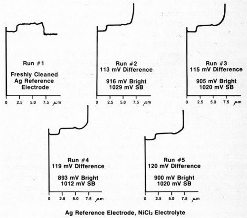
Figure 4 - Potential-thickness graphs of five consecutive determinations using a freshly cleaned silver reference electrode and Solution A from Table 1.
Other precautions are necessary when using the silver reference electrode. If the electrolyte contains an active sulfur compound such as NaSCN, the surface of the reference electrode may be "poisoned" and may not respond to voltage changes of less than 200 mV. Consequently, potential differences between nickel layers will not be observed. Safranek3 and DuRose10 have both pointed out that the electrochemical potentials of nickel deposits are severely affected by SO2 and sulfite ion. Hence, it is advisable to avoid electrolytes containing active sulfur compounds, even if a reference electrode other than silver is used. Figure 6 shows three consecutive measurements made immediately after those in Fig. 5 using the same duplex nickel deposit and silver reference electrode. The electrolyte used to generate the graphs in Fig. 6 consisted of 750 g/L NH4NO3 and 90 g/L NaSCN. Only the total deposit thickness could be obtained with this electrolyte. Similar results were obtained using a platinum reference electrode and the thiocyanate-containing electrolyte. If the silver reference electrode becomes contaminated, it may be cleaned by scrubbing with an abrasive such as silicon carbide powder or abrasive paper until it is bright, followed by conditioning as mentioned above.
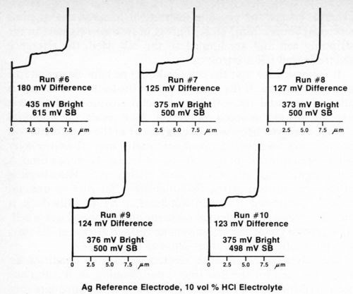
Figure 5 - Potential-thickness graphs of five consecutive determinations after changing to Solution B (10% HCl) from Table 1.
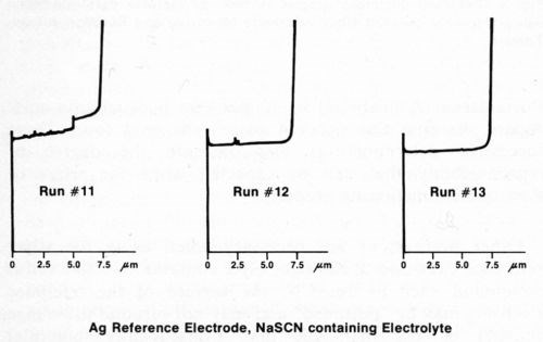
Figure 6 - Potential-thickness graphs of duplex nickel deposit made with NaSCN containing electrolyte (Solution E, Table 1).
When the stripping current is turned on, a potential is observed between the reference electrode and the anode. This voltage is the sum of an impressed potential of fixed value, and a variable voltage which is a function of the anodic dissolution activity of the nickel deposit being stripped. This combined voltage should not be confused with the open circuit potential of the nickel. DiBari17 has shown that the anodic electrochemical activity of nickel is a function of the sulfur content of the nickel. Because sulfur content also influences the open circuit potential, the two values are related and either one can be used as a measure of the activity of the nickels being tested. The electrolyte composition, the anode-to-reference-electrode spacing and the cell voltage are the main variables affecting the value of the fixed potential. Only the electrolyte composition and the electrochemical activity of the nickel have been observed to influence the amount of potential difference measured between nickel layers. A comparison of the absolute potentials shown in Figs. 4 and 5 indicates that there was about a 500 mV shift in potential as a result of changing from the hydrochloric acid electrolyte to the nickel chloride solution, but the potential difference value was not significantly affected.
The open circuit potentials of the nickel layers in a multilayer deposit can be measured, if desired, by turning off the current after stripping has progressed to about the middle of each nickel layer and by electrically isolating the stripping cell from the thickness tester. A relay built into the thickness tester short circuits the stripping cell (anode to cathode) through a resistor when the current is off. As a result, the voltage measured against the reference electrode when the stripping current is off is equal to the combined open circuit potential of the anode and the cathode. A convenient way to electrically isolate the stripping cell from the power supply is to plug a three-conductor ("stereo") phone plug into the "WT" accessory jack on the left side of the thickness tester. Of course, open circuit potentials obtained in this manner will differ from values reported in the literature because the electrolyte and reference electrode differ from those employed by previous researchers.
Experimental results and discussion
Representative samples of typical multilayer nickel deposits were prepared in the laboratory and tested using the procedure described above. Figure 7 shows results obtained for a duplex nickel deposit plated from commercially available semibright and bright nickel baths.** The deposit also had a layer of microporous nickel*** applied over the bright nickel. The figure indicates the thickness and electrochemical potential of each layer.
Hi-Lite this text then type your caption here.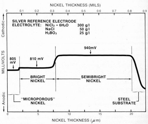
Figure 7 - Potential-thickness graph of a multilayer nickel deposit consisting of semibright, bright and microporous nickel layers.
It is difficult to determine the thickness of a microporous nickel deposit using the microscopic method because it is normally very thin (about 2.5 μm or 0.1 mil) and structurally nearly identical to the bright nickel layer. The electrochemical potentials5 of the microporous nickel and bright nickel also should be nearly identical. However, there often is a small difference between them (5 mV in Fig. 7) that permits a thickness measurement to be made.
Figure 8 is the stripping potential curve obtained for a four-layer nickel deposit. In this case, the deposit was like that in Fig. 7 except that a very active nickel layer† was sandwiched between the semibright and bright deposits. In order for the very active nickel layer to provide the improved corrosion protection it is designed to, it must have a lower potential than, or be anodic to, the other nickel layers. Maintaining the activity of this deposit presents some control problems for the plater, and the procedure described in this paper may provide the easiest way to assess the effectiveness of the total deposit as well as the activity of the very active nickel layer.
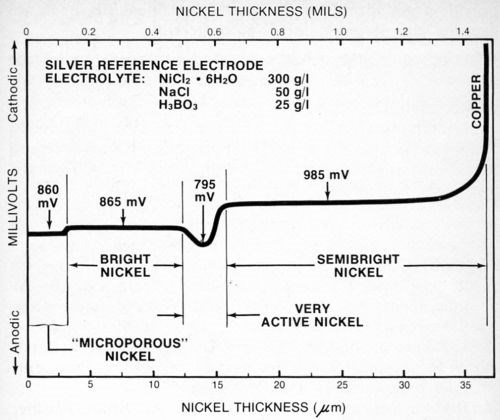
Figure 8 - Potential-thickness graph of a multilayer nickel deposit with a very active nickel layer between the semibright and bright nickel layers.
When the nickel deposit has been stripped through to the underlying metal, the voltage either increases or decreases, depending on the metal and the electrolyte. If the nickel chloride electrolyte is used, the voltage increases if the underlying metal is copper or brass and decreases with respect to the nickel if the basis metal is steel or zinc.
DuRose10 stated that "by the use of different solutions, it was possible to obtain potentials that would place chromium, copper, sulfur-free nickel and bright nickel in any order desired." Consequently, it is important to standardize on one or two electrolytes that give consistent results, place the potentials of the various nickels in the proper order and allow stripping of the deposit to proceed at 100% efficiency. Based on the test results described above, it appears that Formulations A and B in Table 1 meet these requirements. The dilute sodium chloride/cupric nitrate solution suggested by DuRose10 for open circuit potential measurements was found to be unsuitable for use as a stripping solution because of poor anode efficiency. Similar dilute solutions reported in the literature3,10 would be expected to be equally unsuitable.
Using electrolyte A (Table 1) and a silver reference electrode, the greatest potential difference noted to date between the layers of a duplex nickel deposit has been about 155 mV, on a commercially plated part. In spite of a 140 mV potential difference and adequate total deposit thickness, one part failed rapidly in outdoor exposure because of gross cracking in the deposit, suggestive of a highly stressed nickel deposit. This incident emphasizes that adequate deposit thickness and sufficient potential difference are not the only requirements for getting good corrosion protection from duplex nickel deposits. Tensile stress, ductility, metal finishing, cleaning, pitting, dirt inclusions and other factors all can have an adverse effect on the corrosion resistance of the deposit. Assuming that these factors are under control, corrosion of the duplex nickel deposit becomes a function of deposit thickness and potential difference between the semibright and bright nickel layers, whether or not a microdiscontinuous chromium deposit is present.
A significant amount of work is still required to definitively correlate deposit thickness and potential difference with corrosion results, with and without a microporous chromium deposit. However, it appears that a potential difference of 100 mV (using a silver reference electrode and electrolyte A from Table 1) is the minimum value consistent with a good duplex nickel system. The case histories that follow demonstrate that corrosion problems generally are associated with millivolt differences well below 100.
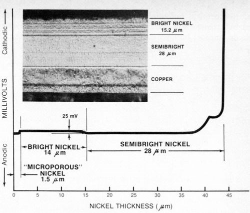
Figure 9 - Potential-thickness graph and photomicrograph (500×) of a defective multilayer nickel deposit. The semibright nickel was anodic to the bright nickel.
Case I - A zinc die-cast automotive grille plated with copper, semibright, bright and microporous nickel, plus chromium, was selected at random from a supplier's shipment and subjected to one cycle of an accelerated corrosion test (Corrodkote, ASTM B-380) which it failed. After stripping the chromium, the total nickel thickness determined with the standard thickness tester was found to be 43.2-μm (1.7-mil) thick, well in excess of the 22 μm (0.88 mil) specified for the part. The nickel deposit was then tested with the modified thickness tester using a silver reference electrode as described above and Solution A from Table 1 as the electrolyte. The resulting potential-thickness graph is shown in Fig. 9. From the graph it was determined that the semibright nickel was anodic to the bright nickel, rather than cathodic as it should be, with an electrochemical potential difference of about 25 mV between the two nickel layers. The thickness of the microporous nickel top-layer was 1.5 μm (0.06 mil) and the bright and semibright nickels were 14 μm (0.55 mil) and 28 μm (1.1 mil) thick, respectively. A sample of the deposit was sectioned, metallurgically polished, etched and photographed (Fig. 9). From the photomicrograph it was determined that the semibright nickel layer was 28 μm (1.1 mil) thick, whereas the bright and microporous layer together were 15.2-μm (0.6-mil) thick, in excellent agreement with the thicknesses obtained from the potential-thickness graph (The microporous nickel layer could not be distinguished from the bright nickel layer in the photomicrograph.). The photomicrograph revealed an atypical non-columnar metallurgical structure for the semibright nickel, which supported the potential data that demonstrated that electrochemically the deposit was not a "true" duplex nickel.
Case II - Automotive bumper-guard samples plated with duplex nickel failed one cycle of an accelerated corrosion test (CASS, ASTM-B 368) even though a sufficiently thick nickel deposit was present. Using the same procedure as in Case I, it was observed that the semibright nickel layer was anodic with respect to the bright nickel by about 28 mV.
The plater carbon treated his semibright nickel bath to remove contaminants that might have affected the electrochemical potential of the deposit. After the bath was carbon treated and additions of recommended additives were made, another bumper guard plated from the purified solution was examined in the same way. This time the semibright nickel layer was 80 mV cathodic with respect to the bright nickel and sample parts passed the accelerated corrosion test. The "STEP"-test procedure verified that the corrective action was beneficial.
One advantage of the procedure described for measuring potential differences between nickel layers is that plated parts can be conveniently tested. Parts that have prematurely failed in service or in accelerated corrosion tests can be checked and the potential difference between nickel layers compared with similar parts that have provided good corrosion protection under similar conditions.
Case III - A number of experimental parts were plated in a production line with semibright, bright and microporous nickel plus chromium. It required three days to plate all the parts in the test program. After mobile exposure in the Detroit area, the parts were returned to the laboratory. Seven of the parts were subsequently checked to determine the potential difference between the semibright and bright nickel layers. Three that had been plated on the first day had an average 88-mV potential difference, one plated on the second day had a 70-mV potential difference, and three plated on the third day had an average potential difference of 53 millivolts. The bright nickel layer was anodic with respect to the semibright nickel in each sample. The corrosion performance of the parts matched the potential differences - the 88-mV parts survived rather well while the 53-mV samples failed. Other variables included in the test had an effect on the overall corrosion results, but the rather significant decrease in the difference of interlayer nickel potential over a short period of plating time demonstrates that a single nickel plating bath can produce deposits of varying potential. Unless adequate controls are maintained, corrosion performance may also vary. Undetected potential variations in duplex nickel deposits may account for some of the poor reproducibility sometimes encountered in corrosion testing of supposedly identical samples. The procedure described in this paper for making thickness, potential and polarity measurements may make it easier to produce multilayer nickel deposits that consistently provide good corrosion protection.
Conclusions
A coulometric method employing a modified commercial thickness tester has been developed to measure the thickness of the individual layers in a multilayer nickel deposit and, at the same time, determine the polarity of each of the nickel layers and measure the electrochemical potential difference between layers. Since the efficacy of duplex nickel deposits is, among other things, dependent on the correct polarity and potential difference between the semibright and bright nickel layers, the procedure provides a means of quickly assessing perhaps the most important elements contributing to the overall corrosion protection of the total deposit. Nickel-plated parts may be tested to predict the degree of corrosion protection provided. Parts that have failed accelerated corrosion tests or prematurely failed in service may be tested easily to determine if the cause of failure was due to thickness or electrochemical potential inadequacies. Initial data suggest that proper deposit polarity and a minimum potential difference of 100 mV (using a silver reference electrode and electrolyte A from Table 1) are required if the superior corrosion resistance of duplex nickel deposits is to be realized. Variations in interlayer potential differences observed in duplex nickel deposits plated from the same baths on successive days indicate that nickel plating baths may deteriorate rapidly due to contamination build up, addition of incorrect or excessive amounts of additives, or poor maintenance, and may account for some of the inconsistent results often encountered in round-robin, corrosion-test programs. The procedure described in this paper should provide a useful tool for the production of multilayer nickel deposits with optimum corrosion protection.
Acknowledgments
The author gratefully thanks Dennis Davidson and Edward Romanowski for their valuable discussions, Charles Isackson for his encouragement and support, and the Chrysler Corp. for permission to publish this paper.
Footnotes
*Model S-77 Thickness Tester, Kocour Co., Chicago, Illinois.
**N2-E and 66, Udylite Division of OMI, Warren, Michigan.
***Dur-Ni, Udylite Division of OMI, Warren, Michigan.
†Tri-Ni, Udylite Division of OMI, Warren, Michigan.
References
1. R.J. Clauss, in Modern Electroplating, 3rd Ed., F.A. Lowenheim, Ed., John Wiley & Sons, Inc., New York, NY, 1974; p. 665.
2. V. Hospadaruk and J.V. Petrocelli, Plating, 48, 479 (1961).
3. W.H. Safranek, R.W. Hardy and H.R. Miller, Proc. Am. Electroplaters' Soc., 48, 156 (1961).
4. J.V. Petrocelli, V. Hospadaruk and G.A. DiBari, Plating, 49, 50 (1962).
5. D.M. Bigge, Plating, 47, 1263 (1960).
6. H. Brown and H. Silman, Trans. Inst. Met. Finish., 42, 50 (1964).
7. Standard B487-73, ASTM, Philadelphia, PA.
8. G. Dubpernell, in Modern Electroplating, 3rd Ed., F.A. Lowenheim, Ed., John Wiley & Sons, Inc., New York, NY, 1974; p. 115. Also, E.M. Baker and W.L. Pinner, Soc. Auto. Eng. J., 22, 331 (1928).
9. J.W. Manquen, Plating and Surface Finishing, 66 (4), 47 (1979).
10. A.H. DuRose, Proc. Am. Electroplaters' Soc., 47, 83 (1960). Also, Potential Measurement of Nickel Deposits, NIPOT0469 (1969), The Harshaw Chemical Co., 1945 E. 97th Street, Cleveland, OH 44106.
11. H.T. Francis, J. Electrochem. Soc., 93, 79 (1948).
12. Standard B504-70, ASTM, Philadelphia, PA.
13. C.F. Waite, Plating, 40, 1245 (1953).
14. P.B. Mathur and N. Karuppanan, Plating, 48, 170 (1961).
15. P.C. Baldwin, Plating, 57, 927 (1970).
16. C.T. Kunze and A.R. Willey, J. Electrochem. Soc., 99, 354 (1952).
17. G.A. DiBari and J.V. Petrocelli, J. Electrochem. Soc., 112, 99 (1965). Also, G.A. DiBari, Plating, 53, 1440 (1966).
About the author

Related Content
Products Finishing Reveals 2024 Qualifying Top Shops
PF reveals the qualifying shops in its annual Top Shops Benchmarking Survey — a program designed to offer shops insights into their overall performance in the industry.
Read MoreLiquid Chrome Vs. Chromic Acid Flake
Contemplating how to continue offering chromic acid services in an increasingly stringent regulatory world? Liquid chrome products may be the solution you’re looking for.
Read MoreHow to Choose Between Sulfate and Chloride-Based Trivalent Chromium
There are several factors to consider when choosing between sulfate and chloride-based baths for trivalent chromium plating. Mark Schario of Columbia Chemical discusses the differences and what platers should keep in mind when evaluating options.
Read MoreAdvantages to Pumped Eductor Agitation
Not all agitation methods are created equally. Pumped agitation with eductor nozzles can improve process tanks and quickly show a reduction in operating costs while keeping staff safe, following environmental legislation and preventing pollution.
Read MoreRead Next
Delivering Increased Benefits to Greenhouse Films
Baystar's Borstar technology is helping customers deliver better, more reliable production methods to greenhouse agriculture.
Read MoreA ‘Clean’ Agenda Offers Unique Presentations in Chicago
The 2024 Parts Cleaning Conference, co-located with the International Manufacturing Technology Show, includes presentations by several speakers who are new to the conference and topics that have not been covered in past editions of this event.
Read MoreEducation Bringing Cleaning to Machining
Debuting new speakers and cleaning technology content during this half-day workshop co-located with IMTS 2024.
Read More


.jpg;maxWidth=300;quality=90)


