Crack Formation during Electrodeposition and Post-deposition Aging of Thin Film Coatings - 9th & 10th Quarterly Report
This NASF-AESF Foundation research project report covers the ninth and tenth quarters of project work (January-June 2018) on this AESF Foundation Research project at the University of Houston. The work continued towards identifying the effective pulse deposition approach to control and mitigate the stress state of chromium thin films and also involved a comprehensive study of palladium stress evolution during electrodeposition and strategies to mitigate its magnitude.
Editor’s Note: This NASF-AESF Foundation research project report covers the ninth and tenth quarters of project work (January-June 2018) on this AESF Foundation Research project at the University of Houston. Access information to past project reports referred to in this paper is listed at the end of this report. A printable PDF version of this report is available by clicking HERE.
Objective: The objective of the proposed work is to study fundamental and practical aspects of crack formation in electrodeposited thin films. The aim is to identify and quantify the key parameters of the electrodeposition process affecting the crack formation in thin films. This study should enable development of an effective strategy generally applicable in practice whenever electrodeposition process for crack-free films is demanded.
The activities in this period continued towards identifying the effective pulse deposition approach to control and mitigate the stress state of chromium thin films. The chromium films were deposited from Cr+3-containing electrolytes (EXDBA 1411 Bath; pH=5) using different pulse functions, and their stress state was compared to the ones deposited with the DC method. In addition to these activities, in this report we show for the first time a comprehensive study of palladium stress evolution during the electrodeposition process and strategies to mitigate its magnitude using a lead UPD monolayer serving as a surfactant and suppressor of the hydrogen evolution reaction.
Personnel:
- Stanko R. Brankovic, P.I., Electrical and Computer Engineering and Chemical and Biomolecular Engineering, University of Houston,
- Kamyar Ahmadi, Ph.D. Student, Material Science Program, University of Houston,
- Miad Yarali, Ph.D. Student, Material Science Program, University of Houston.
- Omer Faruk Karadavut, M.S. student, Electrical Engineering Department, University of Houston
Experimental approach and results
Chromium pulse deposition approach for stress control.
In this period, activities towards identifying an effective pulse current function design were continued (see previous report for prior art). The analytical work based on the diffusion equation solution to estimate the off-time during the pulse current deposition, discussed in the previous report, was abandoned. The reason for this was that the predictability of the mathematical estimates was very dependent on the choice of arbitrary parameters, such as the hydrogen diffusivity in the chromium matrix, which could not be reliably adapted from the literature. For this reason, a different approach was considered, where the estimate of the off-time was based on the analysis of the stress transients during the relaxation after short periods of DC deposition. This allowed us to study the kinetics of hydride decomposition as the main signature of the tensile stress relaxation and to fit the model to the experimental data to extract the rate constant of the hydride decomposition reaction. This parameter was then used for the design and estimate of the off-time in the pulse current deposition function. The full analytical model used for the analysis of the stress transients during relaxation in solution will be presented in an upcoming publication. In this report, we focus our discussion on presentation of the stress evolution data during the pulse deposition. This data demonstrates clearly that the stress state in the chromium films can be qualitatively changed from compressive to tensile by an effective design of the off-time during the pulse current deposition.
In Fig. 1(a), the stress transients during the DC and pulse current depositions are presented. The duration of the on-time during the pulse function is 1 sec, while the off-time varies from 0 (DC deposition) to 1 sec, (50% duty cycle). The overall duration of the experiment was adjusted so that the ultimate thickness of the chromium films was the same for each set of data. The pulse current used in these experiments was 350 mA/cm2. As one can see, DC deposition, and pulse current with very short off-times (97%, 95%, 93%, 91% duty cycle) produce a deposit which has a negative (i.e., compressive) state of stress (F/w). The net stress state for the 91% duty cycle is close to zero, and thus it is considered to represent a stress-free chromium film. For pulse functions that have a lower duty cycle than 91%, the stress state in the chromium film changes to a positive, i.e., tensile state. The final stress state in the chromium films as a function of the off-time duration is shown in Figure 1(b). This data shows a qualitatively different stress state than what has been so far encountered in our studies during the chromium film deposition from the Cr+3-based electrolyte (compressive). Moreover, the tensile stress is characteristic of as-deposited chromium films from Cr+6 baths, and these results are of significant value. It seems that the sufficient rest time in the pulse function cycle, which allows the total breakup of the hydride phase in the grown layer, produces chromium films with the positive stress state. This indicates that the grain zipping phenomenon is dominant and is the stress-determining process as compared to hydride formation. Therefore, we expect that the higher positive stress state in the chromium films, such as those produced by a 50% duty cycle, indicates the low amount of trapped Cr-hydride. These films are expected to have much lower propensity for cracking during a post-deposition aging and annealing treatment. These evaluations are currently underway and this data will be presented in the next report.
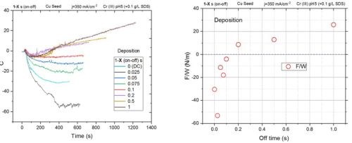
Figure 1 - (a) Force per width transients for chromium films deposited with a pulse current of 350 mA/cm2 and on-time = 1 sec and different values of off-times; (b) Force per width vs. off-time for chromium for transients shown in (a).
Palladium deposition – effective approach and solution design
The most critical issue with the electrodeposition of palladium films is crack formation as a consequence of hydrogen embrittlement1. This problem could be easily circumvented if palladium deposition was conducted at potentials more positive than the hydrogen reversible potential. However, in practice, the choice and stability of substrates often require that the electrodeposition potential is within the hydrogen evolution reaction region (HER). At these potentials, hydrogen absorption into palladium is facile and palladium easily forms hydrides; α-Pd-hydride and β-Pd-hydride. One of the characteristic observations associated with hydrogen absorption into palladium during electrodeposition is a large compressive stress build-up as opposed to tensile stress typically observed during deposition of transition metals. α-Pd-hydride (H/Pd < 0.03) has a slightly larger lattice than palladium (3.889 vs. 3.893 Å) and predominantly forms at potentials where a low overvoltage for HER exists. In this case palladium films do show low stress, and generally these conditions produce crack-free palladium films. However, if the overvoltage for HER is large, both hydrides can form with increasing predominance of β-Pd-hydride at larger overvoltages for HER. β-Pd-hydride (H/Pd > 0.56) has a much larger lattice constant than palladium (3.889 vs. 4.04 Å), and as it forms during the palladium deposition, it exerts a large compressive stress on the palladium film matrix. This hydride is unstable and, upon termination of the deposition process, transforms into α-Pd-hydride, releasing a large quantity of hydrogen and generating a huge tensile relaxation (aging stress). This leads to palladium film cracking.
The work and results presented here focus on developing a new approach to electrochemical synthesis of crack-free palladium films. In this approach, lead (Pb) underpotentially deposited (UPD) on the palladium surface, with monolayer or submonolayer coverage, serves as a mediator, surfactant and hydrogen evolution suppressor. The general approach for solution design is that the lead ion concentration is always equal to or larger than the palladium ion concentration (Pd+2 or Pd+4). This means that the lead UPD process will always be faster than palladium deposition, ensuring that the palladium surface is instantly covered by a lead layer as soon as the new palladium nucleus is formed. Several solutions were examined and the results for two of them are presented here.
Solution #1: 10-3M Pd+2 + 10-3M H+. To explore the stress state of a palladium film grown with various applied potentials, the stress (force/width) of the film during multi-step potentiostatic deposition was recorded. In this measurement, the deposition potential was changed from +0.6 to -0.6 V with intervals of 0.1 V, sequentially after 40 sec deposition at each potential.
As shown in Fig. 2, the film experiences tensile stress at potentials more positive than -0.2 V. The tensile stress in the film can be associated with the formation and merging of palladium grains (grain boundary zipping). However, at potentials more negative than -0.2 V, the film exhibits compression. These potentials are close to the calculated reversible potential1 for proton reduction (HER: -0.36 V). Exceeding the HER potential, the film undergoes a significant compression, which suggests that Pd-H forms at potentials below -0.2 V.
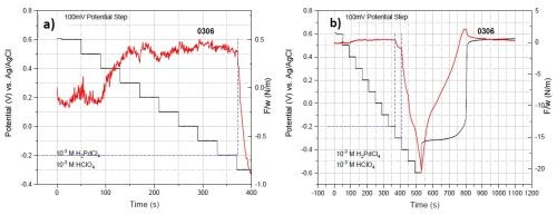
Figure 2 - Force/width data of multi-step potentionstatic depositions for solution #1. The black and red plots show the potential and F/w transients, respectively. The first applied potential is +0.6 V and with potential drops by 0.1 V at intervals of 40 sec.
Multi-step deposition qualitatively gave us the stress state of the palladium film grown at various potentials. However, presence of the residual stress from deposition in a previous potential step and also the short deposition time at each potential made quantitative comparison of the stress state of the films as a function of applied potentials impossible. For the quantitative comparison, we potentiostatically deposited palladium films at each potential on a stress-free cantilever for a constant amount of time (150 sec). To make the cantilever stress-free, after deposition in each potential, the grown film was stripped by applying a high enough positive potential (0.8-0.9 VAg/AgCl). To ensure completion of the stripping we followed three steps:
- Monitoring the stripping current to the reach minimum/steady state,
- Monitoring the F/w data during the stripping to reach the d(F/w)/dt ≈ 0,
- Visual examination of the cantilever in the solution.
As an example, Fig. 3 shows the F/w transient of a film deposited at 0.0 V for 150 sec followed by stripping at +0.8 V. During the deposition time, the film developed a tensile stress, which was removed through the film stripping process.
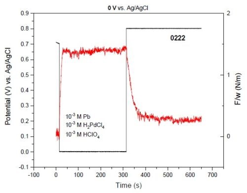
Figure 3 – F/w transient during 150-sec deposition at E = 0.0 V and the film stripping at E = +0.8 V. The black and red plots represent potential and F/w, respectively.
Once the stripping was completed, we applied the next potential with no change in the position of the cell and cantilevers. Figs. 4(a) and (b) show the F/w transients of films deposited at various potentials. Figure 4(c) compares the F/w values at those potentials after 150 sec of deposition. To reproduce the data, we ran the entire set of experiments twice. Figure 4(d) shows the two sets to be in remarkable agreement. As one can see from Fig. 4 and the previous multi-step measurement (Fig. 2), the film exhibits compression at a potential below -0.2 V (orange strip highlighted in Fig 4(d)). Considering the calculated reversible potential of hydrogen (-0.36 V), HER, as the source of hydrogen for Pd-H formation, it would not be expected between -0.2 and -0.36 V. This expectation is considered along with the data of the current (I) transient for the potentiostatic depositions (Fig. 5). The sudden jump of the current value observed at -0.4 V implies that the overpotential of HER is exceeded after -0.35 V. Accordingly, a slight compression below -0.2 V can be related to the formation of hydrogen UPD on the surface of the depositing palladium. Based on our previous measurements, hydrogen UPD on the palladium surface starts at 0.15-0.18 V underpotential (vs. 2H+/H2). This means that between -0.2 to -0.36 V, a (sub)monolayer of hydrogen adsorbs on the surface. The system is dynamic and continuous deposition of palladium brings fresh palladium on top. Therefore, additional hydrogen would sit on this surface and absorption of hydrogen at a potential more positive than the reversible potential of hydrogen occurs continuously.
Exceeding the overpotential for HER, however, provides a significant amount of hydrogen and drive for Pd-hydride formation. This is shown in Fig. 4, where a high surface concentration of hydrogen due to HER causes a huge compression in the film. This originates from two phenomena: first, with more hydrogen, more Pd-H forms and incorporates in the palladium matrix. Second, at a high concentration of hydrogen, Pd-H forms beta phase (β-PdHx) with a lattice constant of 4.03 Å. This value is much larger than that of pure palladium, which puts the palladium matrix in even more compression.
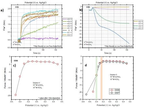
Figure 4 – Stress state of films deposited with various potentials from solution #1. F/w transients of the films deposited with potentials in range of (a) +0.5 to -0.2 V and (b) -0.2 to -0.5 V; (c) values of F/w at 150 sec (last moment of deposition) for various potentials; (d) comparison of final values of F/w for two sets of measurements.
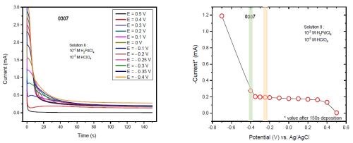
Figure 5 - (a) Current (I) transient at various potentiostatic depositions; (b) values of current at 150 sec for various potentiostatic depositions extracted from plot (a). Note that the increase in current at -0.4 V is likely rooted in HER.
Solution #2: 10-3M Pd+2 + 10-3M H+ + 10-3M Pb+2. Lead is known to suppress hydrogen evolution and it is generally known as a catalyst poison for HER. This means that a monolayer of lead UPD over a growing palladium film can serve the purpose of HER suppression. To find the potential for formation of a lead UPD layer on a growing palladium film, we employed our electrochemical quartz crystal microbalance (EQCM) system. The EQCM enabled us to measure the mass change of the deposit during cyclic voltammetry (CV). In this system, a gold coated quartz crystal oscillates at 6 MHz frequency. Through the deposition, the crystal becomes heavier and therefore the frequency drops accordingly. From the change in frequency, the mass of deposit can be calculated. This system is able to measure mass change in the range of nanograms. Figure 6 shows the main part of our EQCM set-up.

Figure 6 – EQCM set-up configuration: (a) gold-coated quartz crystal and its position in the EQCM cell (3 ml) and (b) EQCM cell as connected to the oscillator.
Figure 7 shows the simultaneous plots of current response and mass change of the palladium film during the potential sweep (cyclic voltammogram). The large deposition and stripping peaks are mainly due to the deposition of palladium. Below 0.0 V, a weak cathodic peak is apparent. This peak is in the underpotential region of both lead and hydrogen. A closer look at the frequency change before and after the peak is done to reveal the origin of the peak. Based on our previous measurements, a monolayer of lead changes the frequency by an order of 20 Hz. However, this peak does not affect the frequency value. This implies that the peak originates from hydrogen UPD, where the mass change is negligible and below the sensitivity of our EQCM. Based on this measurement, we were not able to distinguish any peak for lead UPD.
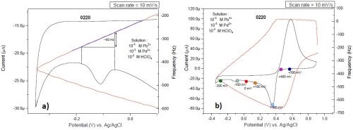
Figure 7 - Cyclic voltammogram of solution #2 and the frequency change obtained during EQCM experiments: (a) magnified detail of part of the voltammagram in (b).
On the other hand, elemental analysis of the films deposited at various potentials shows the presence of lead even at a +0.3 V deposition potential. This means that lead is codeposited with palladium starting at > 0.7 V underpotential (Fig. 8). Lead-palladium underpotential codeposition has not been reported in the literature and needs detailed study.
Figure 8 shows a sudden increase in the atomic percentage of lead in the deposit at -0.5 V (from 25% to 60%). This jump originates from the fact that -0.5 V sits below the reversible potential of lead (-0.42 V) where overpotential deposition (OPD) of lead occurs. Current transient data (Fig. 9) also indicates that a major increase in the current occurs below -0.4 V where OPD of lead starts.
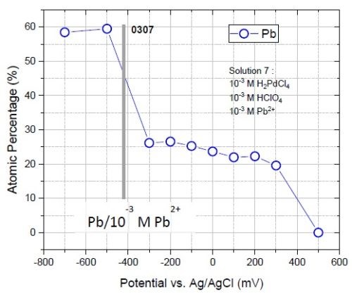
Figure 8 - Atomic percent of lead in the film deposited from solution #2 at various potentials. The onset of overpotential deposition is shown by a solid line.
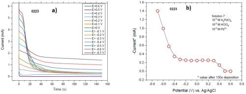
Figure 9 - (a) Current transient of the films deposited from solution #2 on the cantilever at various potentials; (b) the value of the current at the last moment of deposition (150 sec).
We also performed in-situ stress measurements with the same procedure as used for solution #1 to investigate the effect of lead on the stress in the palladium film. The addition of 0.001M Pb+2 in the solution significantly reduces the compression in palladium film. Figure 10 shows the multi-step deposition of the palladium film deposited from solution #2. The net stress of the film at even high overpotential for reduction of proton is tensile. This means that presence of the lead in the film clearly suppresses the Pd-H formation and changes the sign of the stress in the palladium films. This is the proof of the concept for our approach that lead UPD on growing palladium can be used to suppress HER and Pd-hydride formation and form palladium films with tensile stress at potentials more negative than HER. However, the presence of lead in the palladium films, and the newly discovered phenomenon of underpotential Pb-Pd co-deposition requires that this system be investigated in more detail.
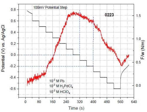
Figure 10 - F/w data of multi-step potentiostatic deposition for solution #2 contains 10-3M Pb+2. The deposit does not exhibit compression even after deposition at -0.6 V for 40 sec.
Figure 11 shows stress measurement data of the palladium films deposited from solution #2 at various potentials. We have done two sets of measurements with 150 and 300 sec deposition, Figs. 11(a, b and c). Figure 11(c) compares the stress values of these two measurements at the very end of the deposition experiments. The data shows a very good match, since the F/w values of the films over the deposition-time have already reached a steady state before 150 sec. Figure 11(d) compares the stress data of solution #2 with that of solution #1. Clearly, the addition of lead in the solution dramatically reduces the compression even at the high overpotential for HER, where the palladium films experience only a slight compression. Now, the question is how the presence of a larger quantity of lead ions in the system will change the elemental composition and stress-state of the film, i.e., what is the optimum solution design in terms of lead ion content. These questions are the topic of our current research towards finding the optimum solution design which will lead to low stress palladium films with a minimum content of lead deposited at large overpotentials for HER.
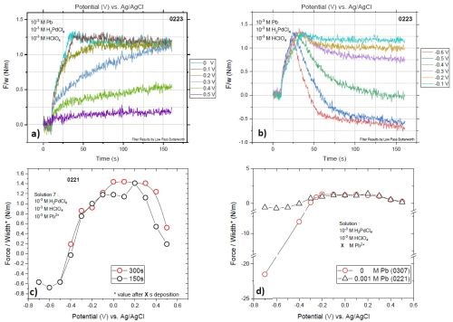
Figure 11 - Stress state of films deposited at various potentials from solution #2: F/w transients of the films deposited with potentials in range of (a) +0.5 to 0.0 V and (b) -0.1 to -0.6 V; (c) comparison of the final values of F/w for the two sets of measurements with 150 and 300 sec of deposition; (d) comparison of the F/w values as a function of deposition potentials for solutions #1 and #2.
Conclusion
In this period, significant progress in understanding the stress control in chromium deposit has been made. Finally, we can say that we do control the stress state and stress sign in chromium films at will by choosing the appropriate pulse deposition function. The question remains as to which stress state, very tensile or close to zero, is desirable when the mechanical properties and structure of chromium films are evaluated. These measurements are currently under way and will be reported soon. The progress in understanding the stress and stress control in palladium films is the new topic of our research which has been introduced in this report. The idea of using lead as an HER and Pd-hydride suppressor seems to yield positive results. However, complications do exist, due to the existence of Pb-Pd underpotential co-deposition, which is a phenomenon unreported until now. This fundamental effect renders a lead UPD monolayer approach, yielding palladium films with some lead content which might limit their application even if the stress state in palladium films is desired and ensures their structural integrity. We are currently exploring work on an optimum solution design which will yield palladium films with minimum lead content and an acceptable level of compressive stress.
Reference
1. J.A. Abys, Modern Electroplating, Chapter 12- Palladium Plating, M. Paunovic and M. Schlesinger, Eds., John Wiley and Sons, Inc (2010); p. 327.
Past project reports
1. Quarter 1 (January-March 2016): Summary: NASF Report in Products Finishing; NASF Surface Technology White Papers, 81 (2), 12 (November 2016); http://short.pfonline.com/NASF16Nov2.
2. Quarter 2 (April-June 2016): Summary: NASF Report in Products Finishing; NASF Surface Technology White Papers, 81 (3), 14 (December 2016); http://short.pfonline.com/NASF16Dec2.
3. Quarter 3 (July-September 2016): Summary: NASF Report in Products Finishing; NASF Surface Technology White Papers, 81 (4), 12 (January 2017); http://short.pfonline.com/NASF17Jan2.
4. Quarter 4 (October-December 2016): Summary: NASF Report in Products Finishing; NASF Surface Technology White Papers, 81 (8), 16 (May 2017); http://short.pfonline.com/NASF17May2.
5. Quarter 5 (January-March 2017): Summary: NASF Report in Products Finishing; NASF Surface Technology White Papers, 81 (11), 12 (August 2017); http://short.pfonline.com/NASF17Aug1.
6. Quarter 6 (April-June 2017): Summary: NASF Report in Products Finishing; NASF Surface Technology White Papers, 82 (4), 10 (January 2018); http://short.pfonline.com/NASF17Jan1.
7. Quarters 7-8 (July-December 2017): Summary: NASF Report in Products Finishing; NASF Surface Technology White Papers, 82 (9), 10 (June 2018); http://short.pfonline.com/NASF18Jun1.
About the author

Dr. Stanko R. Brankovic is an Associate Professor in the Electrical & Computer Engineering and Chemical & Biomolecular Engineering Departments, as well as Associate Director, Center for Integrated Bio and Nanosystems at the University of Houston, Houston, Texas. He holds a B.E. in Chemical and Biochem. Eng. from the University of Belgrade, Serbia (1994) and a Ph.D. in the Science and Eng. of Materials from Arizona State University, Tempe, AZ (1999). He is active in many professional societies, including serving as Vice-Chair and member of the Electrodeposition Division Executive Committee of The Electrochemical Society (2006‐present) and as the Chair of the Electrochemical Material Science Division, The International Society of Electrochemistry (2012‐present). His research interests include electrodeposition, thin films, electrocatalysis, sensors, corrosion and electrochemical material science and nanofabrication.
*Corresponding author:
Dr. Stanko R. Brankovic
Associate Professor
Department of Electrical & Computer Engineering
Department of Chemical & Biomolecular Engineering
Department of Chemistry
N 308 Engineering Building 1
Houston, Texas 77204-4005
Phone: (713) 743-4409
Fax: (713) 743-4444
E-mail: srbrankovic@uh.edu
1 Calculation based on the Nernst Equation.
Related Content
An Overview of Electroless Nickel Plating
By definition, electroless plating is metal deposition by a controlled chemical reaction.
Read MorePossibilities From Electroplating 3D Printed Plastic Parts
Adding layers of nickel or copper to 3D printed polymer can impart desired properties such as electrical conductivity, EMI shielding, abrasion resistance and improved strength — approaching and even exceeding 3D printed metal, according to RePliForm.
Read MoreHow to Maximize Nickel Plating Performance
The advantages of boric acid-free nickel plating include allowing manufacturers who utilize nickel plating to keep up the ever-changing regulatory policies and support sustainability efforts.
Read MoreA Chromium Plating Overview
An overview of decorative and hard chromium electroplating processes.
Read MoreRead Next
Delivering Increased Benefits to Greenhouse Films
Baystar's Borstar technology is helping customers deliver better, more reliable production methods to greenhouse agriculture.
Read MoreEpisode 45: An Interview with Chandler Mancuso, MacDermid Envio Solutions
Chandler Mancuso, technical director with MacDermid Envio discusses updating your wastewater treatment system and implementing materials recycling solutions to increase efficiencies, control costs and reduce environmental impact.
Read MoreA ‘Clean’ Agenda Offers Unique Presentations in Chicago
The 2024 Parts Cleaning Conference, co-located with the International Manufacturing Technology Show, includes presentations by several speakers who are new to the conference and topics that have not been covered in past editions of this event.
Read More





.jpg;maxWidth=300;quality=90)

