Nanoporous Anodic Oxides: Fabrication, Applications, Sensing and Biosensing
Numerous metals are subjected to anodic oxidation. As a result, one can obtain amorphous barrier-type oxides, crystalline barrier-type oxides or amorphous nanoporous oxides. This paper provides details of sensing techniques and recent advances in the development of NAA-based sensing and biosensing technologies.
Editor’s Note: This paper is a peer-reviewed and edited version of a paper delivered at NASF SUR/FIN 2018, in Cleveland, Ohio on June 4, 2018, in Session 5, Light Materials: Treatments Optimizing Performance. A printable pdf of this paper can be accessed and printed HERE. The slide presentation delivered by Dr. Ventura is available HERE.
ABSTRACT: Numerous metals are subjected to anodic oxidation. As a result, one can obtain amorphous barrier-type oxides, crystalline barrier-type oxides or amorphous nanoporous oxides. Currently, highly ordered nanoporous anodic aluminum oxide (AAO), is obtained with various electrolytes to form nanostructures with a wide range of geometrical features. It allows applications for this material as a template for nanofabrication for a variety of nanowires, nanotubes and nanodots. Also, other anodic oxides have attracted the attention of researchers. For example, anodic titania is currently applied as a key material in dye sensitized solar cells ( DSSC). Anodic titania has also been found to be an efficient catalyst for water splitting and carbon dioxide removal. Further, anodic zirconia nanotubes can serve as efficient support for surface Enhanced Raman Spectroscopy. This paper provides detailed fundamentals of sensing techniques and recent advances in the development of NAA-based sensing and biosensing technologies.
Introduction
Anodization of aluminum has become one of the most popular processing methods to form porous structures with pore diameters ranging from about 10 to over 200 nm. The aluminum anodization process leading to a porous structure is usually performed in electrolytes containing sulfuric, oxalic or phosphoric acid. The structural features of the porous alumina film include pore diameters, interpore distance and porosity and they strongly depend on the chosen electrolyte and anodizing potential.
Porous alumina membranes of anodic aluminum oxide (AAO) are widely used for the fabrication of various nanostructures and nanodevices. Over the last decade many materials, including nanowires, nanotubes and nanodot arrays have been fabricated by the deposition of various metals, semiconductors, oxides and polymers inside the pores of AAO membranes (Fig. 1).

Figure 1 - Schematic diagram showing the typical AAO structure and the major applications for this nanostructured material.
Nanoporous substrates such as porous silicon, nanoporous anodic alumina (NAA), titania nanotube arrays, and track-etched porous polymer membranes have been commonly employed as substrates for advanced sensing devices. NAA processes yield unique structural, chemical, optical, thermal and mechanical properties and biocompatibility besides controllable geometry and exploitable surface chemistry.
Owing to these properties, NAA has emerged as an attractive material for development of sensing tools for chemicals relevant to industry, environment and biomedicine. NAA has been coupled with a wide range of optical and electrochemical techniques such as photoluminescence (PL), surface plasmon resonance (SPR), surface enhanced Raman spectroscopy (SERS), reflectometric interference spectroscopy (RIS) and electrochemical impedance spectroscopy (EIS) (Fig. 2).
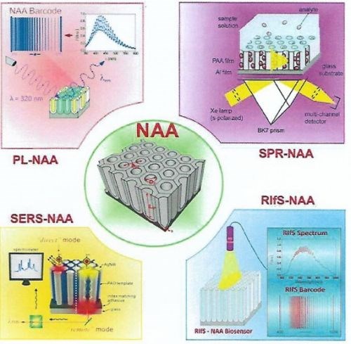
Figure 2 - Schematic diagram showing all four optical sensing techniques coupled with NAA for developing highly sensitive optical sensors.
Photoluminescence
Photoluminescence (PL) is a commonly used term for the phenomenon of absorption of radiation energy and emission of light by materials. Absorption of energy from radiation by a luminescent center results in excitation of an electron to a higher energy level, which emits / releases energy in the form of light during the process of returning to the ground state.
Therefore, photoluminescence spectroscopy-based sensing and bio-sensing devices occupy a prominent place among optical devices, due to their excellent sensitivity on emission of light from NAA while passing a positive potential through an aluminum / oxide / electrolyte system against an iridium cathode.
Galvanoluminescence (GL) from a nanoporous anodic aluminum oxide is influenced by parameters, including the nature of the electrolyte (organic or inorganic), the metal surface properties, the purity and pretreatment, and the anodization conditions of temperature, concentration, current density and voltage.
The galvanoluminescence increases with higher temperature, concentration, voltage and current density, as shown in Fig. 3). This is due to an increase in the number of electrons in the excited state increasing with the electrolyte concentration, temperature, current density and voltage.
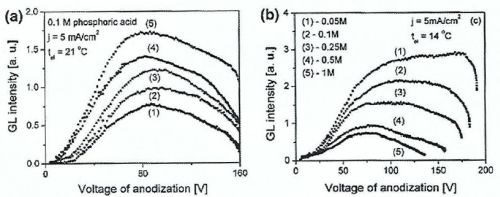
Figure 3 - GL intensity plots for NAA displaying intensity of GL versus voltage for (a) different annealing temperatures: (1) 75°C, (2) 150°C, (3) 250°C, (4) 350°C, (5) 450°C; and (b) varying electrolyte concentrations.
However, the generally accepted mechanism behind PL in NAA is thought to be the presence of impurities and inherent defects of Al2O3 forming NAA. These flaws in the chemical structure of NAA are also referred to as photo-luminescent field centers. There are different types of PL field centers, depending on the type of oxygen vacancies within the impurities.
Similar to galvanoluminescence, photoluminescence, is also influenced by such anodization parameters as anodization, voltage, electrolyte, thermal treatment and pore widening time. Along these lines, the PL intensity for NAA fabricated using a phosphoric acid electrolyte has been studied. As mentioned above, the main contribution to PL of NAA is from the oxygen-containing species. Post anodization thermal treatment and pore widening of NAA display similar trends in PL intensity, which initially increases but decreases after a critical point.
The major advantage of NAA-based PL sensing devices is that, unlike other materials, such as porous silicon, the PL spectrum remains stable without any passivation process.
Photo-luminescence sensing using NAA as the substrate can be accomplished through label molecules (i.e., dyes, Q-dots, etc.). Label-based PL sensing generally results in changes in intensity whereas label-free sensors rely on the shift in the peak in its PL spectrum. It has been reported that confinement of luminescent molecules inside the nanopores results in enhancement of the PL. First reports on label-based PL-NAA sensing observed that adsorption of organic dye and proteins results in enhancement in PL. They also found that their PL peak positions, similar to that of dye itself in ethanol solution, but the PL intensity of embedded dye plus hard anodize solution (HAS) is much higher than that of dye alone, which was attributed to the formation of an Al-complex and coexistence of HAS in the NAA pores.
A label-free PL-NAA sensing approach was adopted by Santos, et al., who developed an optical barcode sensing system. Interestingly, interference-like fringes or oscillations related to the effect were observed during label-free PL-NAA sensing, producing an amplification of the PL oscillations by an enhancement of the photoluminescence at wavelengths corresponding to the optical modes of the cavity formed by the air NAA-Al system. The PL spectrum of NAA is within narrow and well-resolved fringes, which are highly useful for bio-sensing purposes. The number, intensity and position of these oscillations can be tuned by modifying the pore length and diameters. Furthermore, these fringes can generate PL barcodes to be used as target fingerprints. PL barcodes enable development of smart optical biosensors for a broad range of analysis.
Surface modification of nanoporous AAO
AAO nanostructuring (Fig. 4) is an active research area focused on the development of new fabrication concepts and the preparation of more complex pore structures with unique properties suitable for diverse applications. We can expect future developments in this field. Template synthesis of metal semiconductor and polymer nanowires and nanotubes appear to be the primary motivation for these studies. However, these sophisticated AAO structures should find applications in other areas including molecular separation and in optics, for example, as narrow-band filters.
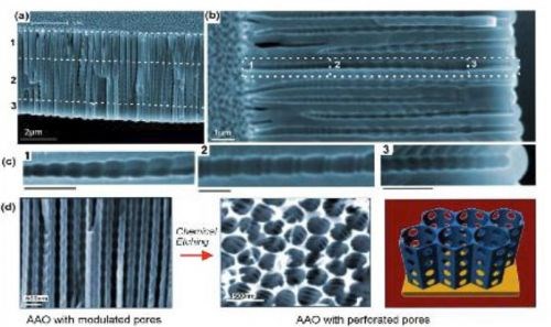
Figure 4 - (a-c) SEM images of AAO with multilayered pore architectures with different pore shapes and structural modulation fabricated by multiple cyclic anodization in 0.1M phosphoric acid with three successive galvanostatic anodization steps by three different cyclic signals; (d) AAO with periodically perforated pores (nanopores with nanoholes) by chemical etching.
In the previous section, we described the recent advances in approaches for structural engineering of AAO to generate new properties and applications. In this section, we will show current research on tuning surface properties of AAO using different surface modification strategies. The surface modifications and functionalization of AAO are expected to significantly expand the scope for applications of AAO-based materials. Furthermore, the effective combination of structural engineering and surface manipulation will underpin a number of emerging applications (e.g., Fig. 5).
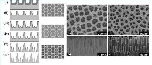
Figure 5 - (Left) Schematic diagram of the sequential fabrication steps of three-tiered branched AAO: (i and ii) first step, first-tier pore anodization and thinning of barrier layer; (iii and iv) second step, second tier formation at reduced potential followed by thinning of the barrier layer; (v and vi) third step, formation of third-tiered pores at further reduced anodization potential and final pore widening; (Middle) corresponding top views of all tiers. (Right) SEM microscopy of the resulting pore structures: (a and b) Top and cross-sectional views of two-tiered branched AAO prepared by combined anodization in 0.3M phosphoric acid (130V) and 0.15M oxalic acid (80V) followed by thinning of the barrier layer; (c and d) Top and cross-sectional views of the three-tiered branched AAO prepared by combined anodization in 0.3M phosphoric acid (130V), 0.15M oxalic acid (80V) and 0.15M oxalic acid followed by thinning of the barrier layer.
The AAO surface is insulating and suffers from chemical instability in acidic environments, which is a disadvantage for some applications. This limitation can be overcome by changing the surface properties and by adding new surface functionalities. The rich content of hydroxyl groups on the AAO surface allow them to be easily altered by modification with organic molecules with the desired functionality. The surface modification techniques that have been explored to improve surface properties and add new functionality to AAO can be divided into two groups: as (1) wet chemical synthesis and (2) gas-phase techniques. The most common approaches for AAO surface modification are summarized as follows. Wet chemical approaches include self-assembly processes (silanes, organic acids, and layer-by-layer deposition), polymer grafting, sol-gel processing, as well as electrochemical and electroless deposition. Subsequent modifications of the introduced functionality with biomolecules of nanoparticles can be carried out. Gas-phase surface modification techniques used for surface modifications of AAO include thermal vapor metal deposition, chemical vapor deposition (CVD), plasma processing and polymerization and atomic layer deposition (ALD). Combinations of these two modification techniques on AAO have also been described, showing the ability to tune surface functionalities and properties of AAO for specific applications.
Complex internal pore architectures
AAO membranes with complex internal pore architectures hold considerable prospects for the development of advanced molecular separation and sensing platforms for use as templates for the fabrication of nanostructured nanowires and nanotubes with unique magnetic, electrical and optical properties. Several approaches have been explored to design modulated pore channels and architectures which include multi-step anodization where the type of electrolyte or electrolyte concentration is changed after each step, changing the electrolyte temperature during anodization, varying the applied voltage or current during anodization or combining anodization and chemical etching.
It is well established that pore diameters in AAO are dependent on the nature of the electrolyte and the applied voltage used during anodization, so the simplest way to alter internal pore geometries would seem to change these two parameters during the etching.
This work sparked extensive interest in the fabrication of hierarchically Y-branched structures. The multiple branched pore structure was fabricated by a combination of reducing the applied voltage by a factor of 1/n (n referring to the number of branches), changing the electrolyte after each anodization step and thinning the barrier layer after each anodization step at the pore bottom by chemical etching. The anodization potential in several steps and applied chemical etching after each step to fabricate the AAO membranes with 3D multi-tiered branch nanostructures as shown schematically in Fig. 6 (Left). Three-tiered branched AAO having an average pore diameter of 275 nm branching into four 125-nm sub-pores in the second tier and four 55-nm sub-pores in the third tier was demonstrated.
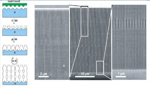
Figure 6 - Long-range ordered AAO membranes with modulated pore diameters: (Left) Scheme for the fabrication of porous alumina with modulated pore diameters by a combination of mild and hard anodization on a pre-patterned aluminum substrate; (Right) SEM micrographs showing the cross-section of the prepared AAO with modulated pore diameters. Magnified cross-section images of the top and bottom parts of the membrane are shown on both sides of the central image.
The variation of anodization conditions by changing electrolytes allows the fabrication of AAO membranes with periodic diameter-modulation in the pore structures combined with the conventional mild (MA) and hard (HA) anodization process to achieve periodic modulation of the pore diameter. The length of each segment was controlled by varying the time of the anodization process. This approach was extended to form shaped pores with nanofunnel geometry. Stepwise anodization processes were used with two different electrolytes, first with phosphoric and followed by oxalic acid. Subsequently, an inverted nanofunnel was obtained by switching the electrolyte sequence. More recently, a method called “pulse anodization” has been developed where both MA and HA processes were applied in the same electrolyte. The method is based an applying long low current pulses (MA regime) followed by short high current pulses (within the HA regime).
Although this method demonstrates the ability to create different pore diameters across the AAO structure, it does not allow control over the pore shape. It has been reported that a new anodization process, termed cyclic anodization, can achieve improved control over the internal pore shape. The concept is based on slow and oscillatory changes of anodization conditions ranging from MA to HA regimes. By changing the period of the current, control over the geometry of pore structures was achieved and AAO with asymmetrical (ratchet-type) and symmetrical (circular) periodic pore geometries, with different lengths, periodicity and gradients, were fabricated. Periodic variations in pore diameter led to photonic crystal behavior in AAO as observed in optical photographs and transmission spectra. The color of the sample and the diffraction peak position in the transmission spectra could be easily controlled by using a chemical post-etching step. Similar results were obtained by fabricating AAO membranes with conical holes. The conical holes were produced by repeating and alternating anodization at 40V and chemical etching with 5% phosphoric acid solution at 20-30°C. Nanosculpturing of AAO membranes with hierarchical pore structures were obtained by applying three different successive cyclic anodization steps: firstly, a cycle with a double-profiled cycle and lastly a series of triangular cycles. SEM images of the resulting AAO membrane showed hierchical and multi-modulated pore structures consisting of three stacked porous layers. Chemical etching led to periodically perforated pores (nanopores with nanoholes).
Surface plasmon resonance (LSPR)
A surface plasmon (SP) is an electromagnetic wave that propagates along the boundary between a dielectric and a metal and behaves likes quasi-free electron plasma. The first report on plasmonic drop on a grating dates back to 1902, but it was thought of as an anomaly in the spectrum. Later, a large drop in reflectivity spectrum when illuminating a thin metal film was noted, but it did not relate to plasmon resonance. However, the drop in the reflectivity spectrum could be correlated to the excitation of surface plasmons, in a different configuration of total internal reflection. It was only in the late 1970s when surface plasmons were employed for the characterization of thin films and monitoring the process at metal boundaries.
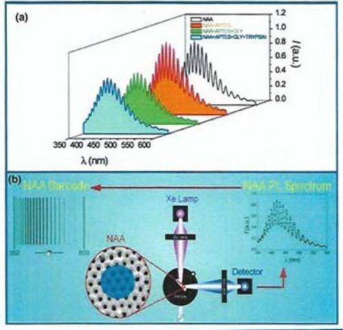
Figure 7 - Biosensor for trypsin: (a) Photoluminescence (PL) spectrum of NAA showing Fabry-Pérot fringes and stepwise changes in PL in the presence of trypsin at the pores; (b) Typical PL setup used for recording luminescence of an NAA substrate along with the Fabry-Pérot fringes that can be converted to PL.
These conditions are successfully satisfied at different wavelengths for several metals of which gold and silver are the most commonly employed in SPR biosensors (Fig. 7). The real and imaginary parts of the propagation constant describe spatial periodicity and attenuation of a surface plasmon in the direction of propagation, respectively. The electromagnetic field of an SP is confined at the metal-dielectric boundary and decreases exponentially into both media. The vast majority of the field of an SP is concentrated in the dielectric, thus the propagation constant of the SP is extremely sensitive to changes in the effective refractive index of the dielectric. After the first study of monitoring a biological reaction in the 1980s, surface plasmon resonance (SPR) was recognized as the most popular analytical method used to probe biological interactions in real time. The advances in SPR techniques over the last three decades have led to the development of SPR systems capable of in situ measurements of a wide range of surface interactions including ligand binding affinity, association / dissociation kinetics, affinity constant, and highly sensitive surface concentration measurements. SPR systems are mainly based on a configuration, where surface plasmons are excited by an evanescent electromagnetic wave generated by the light incident on the surface of a prism coated with a thin layer of metal, mostly gold or silver.
NAA based SPR biosensors are mostly based on a thin metallic film-coated prism configuration. The metal coated prism is subsequently coated with aluminum which is anodized to grow a NAA layer. The surface plasmons of a NAA layer on a prism surface rely strongly on the effective refractive index of the adjacent medium within distances of approximately 200 nm from the metal film.
Surface enhanced Raman scattering spectroscopy (SERS)
The excitation or relaxation of vibrational modes of a molecule result in a change in wavelength that is observed in a photon that undergoes Raman scattering. Every molecule has a different and specific Raman spectrum due to difference in the vibrational energies of the functional groups it contains. However, the intensity of the Raman signal is dependent on the magnitude of polarizability of the molecule which changes with the vibration of functional groups.
Therefore, aromatic molecules display a more intense Raman scattering than aliphatic molecules. The inherent shortcoming of Raman scattering is that its typically an order of magnitude smaller than fluorescence. Therefore, the Raman signal is shadowed by fluorescence emission in most cases. This strong enhancement of Raman signal is most often related to localized surface plasmon resonance (LSPR) that causes enhancement of the local electromagnetic field around a plasmonic nanoparticle / structure. These intense electromagnetic fields induce greater dipole movement in the target Raman scatterer, and accordingly, the intensity of the inelastic scattering increases.
Reflectometric interference spectroscopy (RIFS)
Reflectometric interference spectroscopy (RIFS), is a label-free and highly sensitive optical detection method that is based on the interaction of white light with films on a micrometer scale. In this technique, white light is shined on a thin film and reflected at the two interfaces of the thin film, resulting in amplification of the reflected light signal at wavelengths corresponding to the optical (FP) cavity formed by the thin film-surrounding medium system. Reflectometric interference is very efficiently utilized by nature to provide structural colors to living organisms.
This phenomenon was coupled with synthetic thin films in late 1980. Polymer and metal oxide thin films were fabricated to obtain interference spectrum by monitoring the reflection. The reflection spectrum of these thin films presents intense and well-resolved interference fringes with alternate maxima and minima.
This enhanced inelastic scattering process on enhanced Raman scattering (SERS) on a roughened or organized plasmonic noble metal nanoparticle/substrate detects surface enhancement within the order of 10,000,000 of the typical Raman signal of the target Raman scatterer. This makes SERS an extremely sensitive system for qualitative and quantitative detection of trace amounts of target Raman scattering molecules. NAA has gained huge attention as a substrate for developing SERS-based sensing systems because of its well-defined nanoporous structure, reliable reproducibility, cost-competitive fabrication, high optical transparency, minimal light scattering and large surface area. Similar to LSPR, SERS-NAA devices are also mostly fabricated by evaporating or sputtering a metallic layer of silver or gold on the top bottom side of NAA substrates to generate periodic metallic nanometric structures with controlled geometry. Furthermore, the ability to control and tune the pore structure of NAA enables tuning and optimization of SERS properties of these SERS-NAA substrates at will for specific sensing applications. The SERS enhancement factor G can be calculated to evaluate the enhancement ability of such substrates. The enhancement factor is given by:
G = (Iads/Nads)/(Ibulk/Nbulk)
where Iads is the intensity of a vibration mode in SERS spectrum, and Ibulk is the intensity of the same mode in the normal Raman spectrum. Nads and Nbulk are the numbers of molecules probed in the SERS spectrum and in normal Raman spectrum, respectively.
Raman signal enhancements in the range 1,000,000-10,000,000 range have been reported on NAA substrates decorated with gold and silver nanoparticles grafted onto or in situ synthesized inside NAA nanopores.
For this, the inner surface of a commercially available NAA membrane was first modified with poly-(diallyldimethylammonium chloride) (PDDA), using spin coating followed by incubation with gold nanoparticles approximately 32 nm in size to generate “hot spots” inside the NAA pores (Fig. 8). These SERS-NAA substrates were then employed for the detection of trace amounts of 2,4-dinitrotoluene (2,4-DNT, TNT-based plastic explosive) with modest Raman cross-section. It has been reported that this class of compound is usually not detected by conventional Raman measurements. With this metal nanoparticle-decorated NAA substrate, a Raman signal enhancement on the order of 1.1 x 1,0000,000 was achieved. SERS performance of gold nanoparticle-decorated NAA for the detection of 2,4-DNT was found to be superior. A similar strategy was reported to decorate NAA with silver nanoparticles and the performance of the resulting SERS-NAA substrate was measured by detecting p-aminothiophenol. Pyridine, an important solvent and reagent for pharmaceutical and agrochemical applications was used as a Raman scatterer to probe its sensing performance.
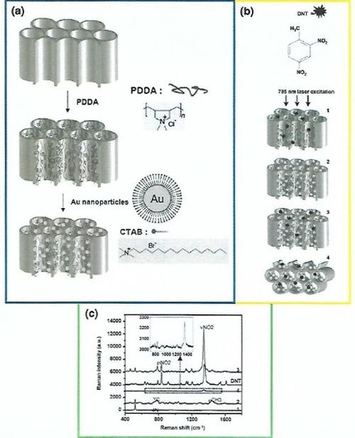
Figure 8 - Schematic diagram demonstrating the procedure for (a) decorating NAA with gold nanoparticles; (b) the chemical structure of 2,4-dinitrotoluene and the schematic of Raman measurement of 2,4-DNT with different laser excitation angles parallel (1,2,3) and perpendicular (4) to the pore axes and (c) the Raman spectrum of DNT powder and 1000 ppm 2,4-DNT on each substrate shown schematically in (b).
NAA-based electrochemical sensors
Electrochemical sensors (Figs. 9 and 10), depending on their principle of detection, can be divided into several types including voltammetric, amperometric and impedometric. Although NAA is inherently insulating, the composite of NAA with electrically conducting materials or redox active species have been successfully used to develop voltammetric or amperometric sensors. NAA, in the form of a membrane after removal of barrier layer, has been used as a flow-through impedometric, capacitive or resistive sensor.
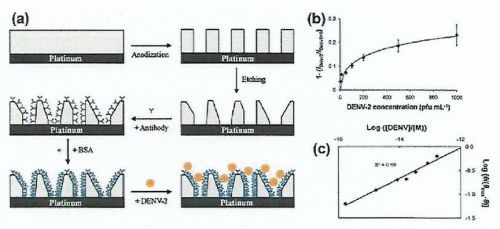
Figure 9 - (a) Design of a NAA-based electrochemical nanosensor for detection of DENV-1 Dengue virus; (b) NAA nanosensor response toward different concentrations of DENV-2 in 0.1M phosphate and (c) its corresponding linear calibration curve in long values.
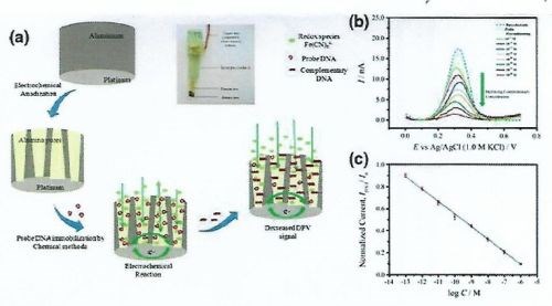
Figure 10 - (a) Construction scheme of NAA-based electrochemical DNA sensors; (b) current-signal response of a bare electrode to increasing concentration of complementary target and (c) its corresponding calibration curve.
Voltammetric and amperometric NAA sensors
Nanoporous anodic alumina can potentially support a large number of capture probes immobilized in its pores due to the large surface area. This is an excellent characteristic for developing membrane type amperometric of voltammetric nano-sensor platforms, which allows higher interaction between the anolyte and capture probe molecules through the pores. As mentioned before, NAA is an electrical insulator, but its pores can be modified with a conductive layer or a redox-active species to transform them into electro-active elements. A composite of NAA with a series of metal or metal oxide depositions (Au, Pt, SnO2), carbon nanotubes (CNT), conductive polymers or other electrochemically active materials, have previously been reported for electrochemical sensing of gas detection (vinyl chloride, ammonia, formaldehyde), glucose, hydrogen peroxide, cholesterol, nucleotides and proteins, enzymatic activity and detection of cells. The electron transfer to the electrode is carried either indirectly via a redox mediator between the NAA substrate and the immobilized molecules or directly by attached conducting linkers using voltammetric and amperometric methods.
The most significant contribution to NAA-based electrochemical sensors has come from the development of a series of NAA-based electrochemical immune-sensors, by growing an NAA layer onto a conducting platinum substrate. The inner surfaces of the NAA-Pt pores were functionalized with antibodies specific to either dengue glucose oxidase. The antibody-antigen reaction was probed by measuring the AC voltammetry signal of a redox indicator. In simple terms, attachment of a specific target molecule inside impedes the diffusion of the redox mediator, therefore resulting in a low voltammetry signal. A three-electrode system was employed which was comprised of a platinum auxiliary electrode, a silver-silver chloride reference electrode and an alumina membrane working electrode. Similar to an antibody-antigen reaction hybridization of complementary target DNA with a DNA probe immobilized inside the NAA pores influences the ionic conductivity of NAA pores. This approach was adopted for the development of a nucleotide biosensor, where the signal was derived from redox across single wire Pt-electrode. Another NAA-membrane based DNA biosensor probes immobilized inside the pores influences the pore size and thus the ionic conductivity of the NAA membrane.
The sensing characteristics of voltammetric and amperometric NAA sensors have been improved by the modification of pores with Prussian Blue (PB) or an iron hexacyanoferrate polymer based on their unique ion-exchange and electrocatalytic properties.
These highly ordered PB arrays act inside NAA as an ensemble of closely packed nano-electrodes, which highly improve the analytical performances of glucose detection by electrocatalytically reducing enzymatically liberated H2O2. The resulting glucose biosensor showed excellent performance with a broad linear concentration range over three orders of magnitude and a low detection limit of 1 μM. Similarly, PB-NAA sensors have been also successfully demonstrated for ion selective detection of Na+ and K+ ions.
This sensor employs selective anodic and cathodic reactions with suitable thermodynamic potentials, considering the reactions taking place at the sensing and auxiliary electrodes, which are modified with appropriate mediators or enzymes (Fig. 11). In this case, the PB nanotubes reduce H2O2 and are reduced themselves by electron flow from the counter reaction taking place at the auxiliary electrode. For highly sensitive detection of dengue virus serotype-2 (DENV-2), the resulting sensor displays an extremely fast reaction time of less than 3 min and outstanding lower detection limit of 0.03 pfu/mL, which is comparable to a conventionally-used PCR setup.
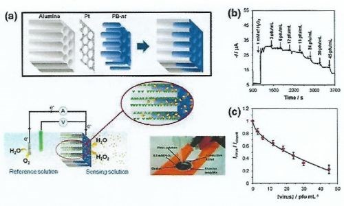
Figure 11 - (a) Schematic diagram showing the process of depositing Prussian Blue nanotubes inside NAA pores and their use for virus sensing; (b) typical closed-circuit steady-state current response of a PB nanotube-based sensor toward DENV-2 virus and (c) its corresponding calibration plot showing normalized closed-circuit steady-state current versus virus concentration.
Impedance, capacitance, conductance and resistance-based sensors
Electrochemical impedance spectroscopy (EIS) has increased in popularity in recent years due to its applicability in determining double-layer capacitance and in AC polarography, characterization of electrode processes and biosensing applications (Fig. 12). EIS studies the system response to the application of periodic small amplitude AC pulses at different frequencies. In simple terms, EIS measures the dielectric properties of a material as result of the interaction of the applied electric field at different frequencies and the generated electric dipolar moment of the material. The removal of the oxide barrier layer from the bottom of NAA pores reduces the electrical resistance and allows ionic current to flow through the pore bottom by reducing the electrical resistance and the flow of ionic current through the pores. Therefore, NAA can act as a flow-through sensor as the attachment of target species onto the capture probe inside the NAA pore hinders the transport of ionic species across the membrane, influencing the electric dipole of the structure. Another advantage of the large internal surface area of NAA pores is its ability to immobilize large amounts of capture probes for binding target species. This bending event can be sensitively detected using impedance measurements.
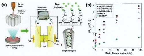
Figure 12 - (a) Schematic diagram of NAA-based impedance sensors for the recognition of streptavidin and biotin interaction with certain areas of pores selectively opened with focused ion beam (FIB) technology; (b) graph showing changes of pore resistance against various concentrations of biotin for the pore areas opened using FIB.
Equivalent circuits based on different models can be generated to fit the experimental data and understand the electric behavior and properties of NAA. NAA-based impedance sensors have been used for the detection and study of DNA hybridization, protein and lipid membrane interactions, cancer cells, viruses and bacteria.
NAA, due to its high thermal stability, surface area and affinity towards gases and vapors, has been used as a substrate to develop gas or humidity sensing devices. A capacitance- and resistance-based chip can be fabricated to measure relative humidity (RH), using NAA layers grown on silicon wafers. Two different sensors, namely: (a) capacitance-based and (b) resistance-based, were fabricated by growing two types of electrodes on the NAA surface (i.e., a vapor-permeable palladium layer and a gold grid). The highest sensitivity of the capacitance-based RH sensors was found to be much higher than most off-the-shelf commercial humidity sensors.
An environmental capacitive sensor based on NAA quantified polychlorinated biphenyls (PCBs), an environmental pollutant. The cylindrical pores of NAA provide a large surface area for the adsorption of PCBs, which in turn can lead to enhancement of capacitive response. PCBs can be adsorbed onto NAA pore walls by simply dropping a methanol solution of PCBs. This simple NAA-based capacitive sensor also displays a good response to PCB even with the presence of a nonspecific interferent like benzene. A parallel place capacitor model was used to understand the behavior of capacitance in the NAA sensor, which shows an exponential increase of capacitance with increasing PCB concentration.
A nanocomposite of NAA with tungsten trioxide was used to develop a resistance-based sensor for toxic gases (i.e., nitrogen dioxide, ammonia and ethanol). This type of sensor also displayed incremental resistance with increasing concentration of the toxic gases.
Apart from gas sensing, NAA-based conductivity sensors have been used to detect DNA hybridization and enzyme activity. The DNA sensor can measure changes in ionic conductance as result of DNA hybridization inside NAA pores. In another study, a NAA-based conductance sensor was used to establish the activity of enzyme immobilized (urease in this case) inside NAA pores. This supports the concept that NAA-based electrochemical sensors can be used for both qualitative and quantitative detection on anolytes or measuring kinetics of an anolyte-receptor reaction or enzyme-substrate reaction.
Summary and conclusions
Over the past several years, significant progress, has been made with regard to structural engineering and surface modification of nanoporous AAO material. Much of this progress has been application-driven. In this review, we have drawn together innovative approaches on controlling and designing structural growth of AAO with different sizes, arrangements, structures, geometries and pore architectures.
Access to these structures is achieved by changing the anodization conditions such as current, voltage and type of electrolyte during electrochemically self-ordering of AAO. Researchers are also pushing the boundaries of molecular separations using AAO with pores of controlled shape and size, internal surface modification and by exploring the effect external parameters, such as, pH, flux concentration gradient and ionic strength.
An excellent consistency between experimental results and theoretical predictions of the interpore distance was observed for the highest studied anodizing time and the highest methanol content in the anodizing electrolyte.
Future reports on structural and chemical modifications of NAA will facilitate the development of even smarter and advanced sensing devices. Finally, we can conclude there is a bright opportunity for development of miniature sensing devices based on NAA as lab-on-a chip systems for point of care diagnostics, industrial and environmental applications.
Bibliography
- R.B. Thompson, Fluorescence Sensors and Biosensors, CRC Press, Boca Raton, FL, 2005.
- A. Santos, T. Kumeria and D. Losic, “Nanoporous Anodic Aluminum Oxide for Chemical Sensing and Biosensors,” TrAC Trends Anal. Chem., 44, 25-38 (2013).
- M.J. Sailor, Porous Silicon in Practice: Preparation, Characterization and Applications, Wiley-VCH, Weinheim, Germany, 2011.
- S. Ikonopisov, “Problems and Contradictions in Galvanoluminescence: A Critical Review,” Electrochim. Acta, 20 (10), 783-793 (1975).
- B. Kasalica, et al., “Nature of Galvanoluminescence of Oxide Films Formed by Aluminum Anodization in Inorganic Electrolytes,” J. Phys. Chem. C, 111 (33),12315-12319 (2007).
- S. Stojadinovic, et al., “The Effect of Annealing on the Photoluminescent and Optical Properties of Porous Anodic Alumina Films Formed in Sulfamic Acid,” Appl. Sur. Sci., 256 (3), 763-767 (2009).
- G. Huang, et al., “Strong Blue Emission from Anodic Alumina Membranes with Ordered Nanopore Array,“ J. Appl. Phys., 93 (1), 582-585 (2003).
- Y. Mei, et al., “Color Centers vs. Electrolytes for Si-based Porous Anodic Alumina,” Phys. Lett. A, 324 (5), 479-483 (2004).
- G. Huang, et al., “On the Origin of Light Emission from Porous Anodic Alumina Formed in Sulfuric Acid,” Solid State Commun., 137 (11), 621-624 (2006).
- Y. Mei, et al., “Nanoscale Islands and Color Centers in Porous Anodic Alumina on Silicon Fabricated by Oxalic Acid,” Appl. Surf. Sci., 230 (1-4), 393-397 (2004).
- M. Pumera, Nanomaterials for Electrochemical Sensing and Biosensing, CRC Press, Boca Raton, FL, 2014.
- G. Jeon, et al., “Electrically Actuatable Smart Nanoporous Membrane for Pulsatile Drug Release,” Nano. Lett., 11 (3), 1284-1288 (2011).
- V. Rai, et al., “Ultransensitive cDNA Detection of Dengue Virus RNA using Electrochemical Nanoporous Membrane-based Biosensor,” PLOS One, 7 (8) ,e42346 (2012): https://www.ncbi.nlm.nih.gov/pmc/articles/PMC3426509/.
- G. Koh, et al., “Development of a Membrane-based Electrochemical Immunosensor,” Electrochim. Acta, 53 (2), 803-810 (2007).
- B.T.T. Nguyen, et al., Membrane-Based Electrochemical Nanobiosensor for the Detection of Virus, Anal. Chem., 81 (17) , 7226-7234 (2009).
- B.T.T. Nguyen, J.Q. Ang and C-S. Toh, “Sensitive Detection of Potassium Ion using Prussian Blue Nanotube Sensor,” Electrochem. Commun., 11 (10),1861-1864 (2009).
- L.P. Wong, Y.Wei and C-S Toh, “Self-powering Amperometric Sensor and Biosensor,” J. Electroanal. Chem., 671, 80-84 (2012).
- Y.Wei, L.P. Wong and C-S Toh, “Fuel Cell Virus Sensor using Virus Capture within Antibody-Coated Nanochannels,” Anal. Chem., 85 (3),1350-1357 (2013).
- l. Wang, et al., “A Novel Electrochemical Biosensor Based on Dynamic Polymerase-Extending Hybridization for E.coli 0157:H7 DNA Detection,” Talanta, 78 (3), 647-652 (2009).
- K. Kant, et al., “Characterization of Impedance Biosensing Performance of Single and Nanopore Arrays of Anodic Porous Alumina Fabricated by Focused Ion Beam (FIB) Milling,” Electrochim. Acta, 139, 225-231 (2014).
- K. Kant, et al., “Impedance Nanopore Biosensor: Influence of Pore on Biosensing Performance,” Analyst, 139 (5),1134-1140 (2014).
- L. Juhász and J. Mizsei, “Humidity Sensor Structures with Thin Film Porous Alumina for On-Chip Integration, Thin Solid Films, 517 (22), 6198-6201 (2009).
- M. Ghrib, et al., “Effect of Annealing on Photoluminescence and Optical Properties of Porous Anodic Alumina Films Formed in Sulfuric Acid for Solar Energy Applications,” Appl. Surf. Sci., 258 (12), 4995-5000 (2012).
- H. Elhouichet, et al., “Energy Transfer in Porous Anodic Alumina/Rhodamine 110 Nanocomposites,” J. Lumin., 132 (9), 2232-2234 (2012).
- R. Jia, et al., “Enhanced Photoluminescence Properties of Morin and Trypsin Absorbed on Porous Alumina Films with Ordered Pores Array,” Solid State Commun., 130 (6), 367-372 (2004).
- T. Turbadar, “Complete Absorption of Light by Thin Metal Films,” Proc. Phys. Soc. London, 73 (1),40-44 (1959).
- R.B. Shasfoort and A.J. Tudos, Handbook of Surface Plasmon Resonance, Royal Society of Chemistry Publishing, London/Cambridge, UK, 2008.
- I. Pockrand, et al., “Optical Properties of Organic Dye Monolayers by Surface Plasmon Spectroscopy,” J. Chem. Phys., 69 (9), 4001-4011 (1978).
- I. Pockrand, et al., “Exciton-Surface Plasmon Interactions,” J. Chem. Phys., 70 (7), 3401-3408 (1979).
- J. Homola, “Present and Future of Surface Plasmon Resonance Biosensors,” Anal. Bioanal. Chem., 377 (3), 528-539 (2003).
- P. Pattnaik, “Surface Plasmon Resonance,” Appl. Biochem. Biotechnol.,126 (2), 79-92 (2005).
- B. Liedberg, C. Nylander and I. Lunstrom, “Surface Plasmon Resonance for Gas Detection and Biosensing,” Sens. Actuators, 4, 299-304 (1983).
- X. Guo, “Surface Plasmon Resonance-Based Biosensor Technique: A Review,” J. Biophotonics, 5 (7), 483-501 (2012).
- M.C. Estevez, et al., “Trends and Challenges of Refractometric Nanoplasmonic Biosensors: A Review,” Anal. Chim. Acta, 806, 55-73 (2014).
- R.J. Green, et al., “Surface Plasmon Resonance Analysis of Dynamic Biological Interactions with Biomaterials,” Biomaterials, 21 (18),1823-1835 (2000).
- T.D. Lazzara, K. Aaron Lau and W. Knoll, “Mounted Nanoporous Anodic Alumina Thin Films as Planar Optical Waveguides, J. Nanosci. & Nanotechnol.,10 (7), 4293-4299 (2010).
- C.L. Haynes, A.D. McFarland and R.P.Van Duyne, “Surface-Enhanced Raman Spectroscopy,” Anal. Chem., 77 (17), 338A-346A (2005).
- D. Cialla, et al., “Surface-Enhanced Raman Spectroscopy (SERS) Progress and Trends,” Anal. Bioanal. Chem., 403 (1), 27-54 (2012).
- R. Kodiyath, et al., “Assemblies of Silver Nanocubes for Highly Sensitive SERS Chemical Vapor Detection,” J. Mater. Chem. A, 1 (8), 2777-2788 (2013).
- L. Velleman, et al., “Raman Spectroscopy Probing of Self-Assembled Monolayers Inside the Pores of Gold Nanotube Membranes,” Phys. Chem., 13 (43), 19587-19593 (2011).
- X. Wang and S. Smirnov, “Label-free DNA Sensor Based on Surface Charge Modulated Ionic Conductance,” ACS Nano, 3 (4), 1004-1010 (2009).
- Z. Yang, S. Si and C. Zhang, “Study on the Activity and Stability of Urease Immobilized Ontonanoporous Alumina Membranes,” Microporous & Mesoporous. Mater., 111 (1-3), 359-366 (2008).
- L.H. Cohen and A.I. Gusev, “Small Molecule Analysis by MALDI Mass Spectrometry,” Anal. Bioanal. Chem., 373 (7), 571-586 (2002).
- Y. Wada, T. Yanagishita and H. Masuda, “Ordered Porous Alumina Geometries and Surface Metals for Surface-Assisted Laser Desorption/Ionization of Biomolecules: Possible Mechanistic Implications of Metal Surface Melting,” Anal. Chem., 79 (23), 9122-9127 (2007).
- M. Sato, et al., “Sensitivity of an Anodically Oxidized Aluminium Film on a Surface Acoustic Wave Sensor to Humidity,” Sens. & Actuators B: Chem., 20 (2-3), 205-212 (1994).
- Y.L. Rao and G. Zhang, “Enhancing the Sensitivity of SAW Sensors with Nanostructures,” Current Nanosci., 2 (4), 311-318 (2006).
- Z. Yang, et al., “Piezoelectric Urea Biosensor Based on Immobilization of Urease onto Nanoporous Alumina Membranes,” Biosens. & Bioelectron., 22 (12), 3283-3787 (2007).
- J. Haruyama, et al., “Coulomb Blockade Related to Mutual Coulomb Interaction in an External Environment in an Array of Single Tunnel Junctions Connected to Ni Nanowires,” Phys. Rev. B, 62, 8420 (2000).
- J. Haruyama, et al., “Mesoscopic Phenomena in Nanoporous Alumina Films: Single Nano-tunnel Junctions Connected to Ni Nanowires and Carbon Nanotubes,” Appl. Surf. Sci., 175-176, 597 (2001).
- R.M. Metzger, M. Sun, G. Zangari & M.Shamsuzzoha, “Magnetic Nanoparticle Array with Ultra-Uniform Length Electrodeposited in Highly Ordered Alumina Nanopores Alumite,” Mat. Res. Soc. Symp. Proceedings, 636D9.33.1 (2001).
About the author
Dr. Xavier Albort Ventura earned his Ph.D.in Chemistry Engineering Industrial from the University of Barcelona Spain. He is a member of the Barcelona International Trade Fair and has organizing responsibility for the Environment Technical Meetings and at the Eurosurfas show. He is an electroplating consultant for more of 50 European companies from various countries, including Portugal, France, Spain, Italy and Germany. He has been an active presenter at SUR/FIN, having given papers since 1987. He has also been an active participant at Interfinish, presenting papers and conducting workshops since 1984. He has published more than 200 papers in Spain, the United Kingdom, France, the United States and Brazil. He was awarded the Sam Wyman Memorial Award at SUR/FIN 2004 in Chicago for the Best Light Metals paper, “Sealing Method for Anodizing Aluminum and Hard Anodizing and a Test to Determine the Seal Quality of Aluminum.”
*Corresponding author
Xavier Albort Ventura, Professor and Consulting
University Politecnic of Barcelona
Spain Research and Development
Technocrom Industrial and Surfaquim
C. Carabela.la La Niña, 22-24 bis
Barcelona, Barcelona Spain 08017
Phone: 34-93-2054036
Mobile: 34-63-9721065
E-mail: xavieralbort@ono.com
Related Content
Innovation in Plating on Plastic
Plating on advanced plastics solution offers improved adhesion, temperature resistance and cost savings.
Read MoreHow to Choose Between Sulfate and Chloride-Based Trivalent Chromium
There are several factors to consider when choosing between sulfate and chloride-based baths for trivalent chromium plating. Mark Schario of Columbia Chemical discusses the differences and what platers should keep in mind when evaluating options.
Read MoreA Chromium Plating Overview
An overview of decorative and hard chromium electroplating processes.
Read MoreProducts Finishing Reveals 2024 Qualifying Top Shops
PF reveals the qualifying shops in its annual Top Shops Benchmarking Survey — a program designed to offer shops insights into their overall performance in the industry.
Read MoreRead Next
A ‘Clean’ Agenda Offers Unique Presentations in Chicago
The 2024 Parts Cleaning Conference, co-located with the International Manufacturing Technology Show, includes presentations by several speakers who are new to the conference and topics that have not been covered in past editions of this event.
Read MoreEducation Bringing Cleaning to Machining
Debuting new speakers and cleaning technology content during this half-day workshop co-located with IMTS 2024.
Read MoreEpisode 45: An Interview with Chandler Mancuso, MacDermid Envio Solutions
Chandler Mancuso, technical director with MacDermid Envio discusses updating your wastewater treatment system and implementing materials recycling solutions to increase efficiencies, control costs and reduce environmental impact.
Read More


