Qualitative Approach to Pulse Plating
In 1986, the AESF published Theory and Practice of Pulse Plating, edited by Jean Claude Puippe and Frank Leaman, the world’s first textbook on pulse plating. A compendium of chapters written by experts in this then-emerging field, the book quickly became the authoritative text in pulse plating. What follows here is the opening chapter, serving as an introduction to the field. Although the field has grown immensely in the intervening 35 years, the reader will find that the material remains a valuable introduction to those looking to advance the field of pulse plating.
by
Jean-Claude Puippe
Steiger Galvanotechnique SA,
Lausanne, Vaud, Switzerland
Editor’s Note: In 1986, the American Electroplaters and Surface Finishers Society (AESF) published Theory and Practice of Pulse Plating, edited by Jean Claude Puippe and Frank Leaman, the world’s first textbook on pulse plating. A compendium of chapters written by experts in this then-emerging field, including the editors, the book quickly became the authoritative text in pulse plating. What follows here is the opening chapter, serving as an introduction to the field. Although the field has grown immensely in the intervening 35 years, the reader will find that the material remains a valuable introduction to those looking to advance the field of pulse plating. A printable pdf of this article can be downloaded HERE.
1. Introduction
In electrolysis, in contrast to chemical synthesis, one can easily control the reaction rate of a system by working at a given current density, or easily select the magnitude of the driving force for the reaction by adjustment of the electrode potential. Modern electronics has greatly enhanced this inherent advantage of electrolysis by allowing current or voltage to be applied as almost any function of time. Pulse plating takes full advantage of this possibility. There are quite a number of variations, some of which are schematically represented in Fig. 1. Typical waveforms include cathodic pulse followed by a period without current and/or by an anodic pulse; DC with superimposed modulations; a train of cathodic pulses followed by a train of anodic pulses; galvanostatic or potentiostatic pulses; square-wave or modified sine-wave pulses. It should be noted, however, that owing to the fundamental nature of the phenomena involved in the deposition process one cannot make full use of the range of conditions that would be allowed by modern electronics. There are two main limiting factors: the charging of the electrical double layer at the metal-electrolyte interface and the mass transport considerations.
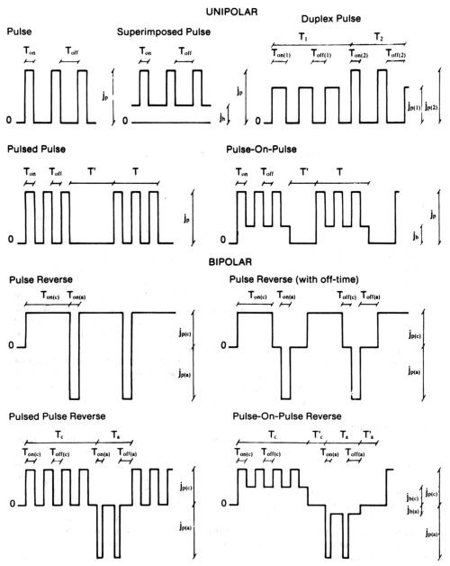
The parameters shown in this figure are independent. The average current density, jm, the dependent parameter, can be calculated from the above mentioned parameters. Pulse reverse is characterized by three different average current densities: jm, jm(c), jm(a), with jm = jm(c) + jm(a).
Figure 1 - Schematic representation and suggested nomenclature for some square-wave modulated current systems, and definition of related parameters.
2. Capacitance effects
The electrical double layer at the electrode-solution interface can be approximated to a plate capacitor with an interplate distance of a few angstroms and therefore with a high capacitance. Charge must be provided to this double layer in order to raise its potential to the value required for metal deposition at the rate corresponding to the applied pulse current which is supplied by the generator. The electrode behaves like a capacitor with a resistance in parallel as schematically represented in Fig. 2, the resistance being a function of the current density. The charging of the double layer requires a certain time, which depends on the current density and on other physico-chemical parameters of the system. For practical purposes, the charging time should be much shorter than the pulse duration, otherwise the current pulse is strongly distorted. Moreover, the time required for discharge of the double layer should be much shorter than the off-time between two pulses. In an extreme case, where the charging and discharging times of the double layer are much longer than the on-time and off-time of the pulse respectively, the pulsed current is virtually a direct current and the term "pulse plating" is hardly applicable. The current required at the beginning of the pulse for charging the electrical double layer is not lost for the metal deposition, since the charge is recovered at the end of the pulse while the capacitor is discharging.
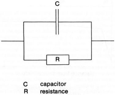
Figure 2 - Equivalent circuit of an electrode.
Pulses in a frequency range where capacitive effects are relevant do not significantly influence the current efficiency but affect the amplitude of the pulse and hence the energy of the electrodeposition reaction. In fact, the potential benefit of pulse plating, for example, in influencing the structure and therefore the properties of deposits, is lost. In most cases the user of pulse plating should therefore avoid working with on- and off-times shorter or of an order of magnitude comparable with the charging or discharging time of the double layer.
3. Mass transport effects
The limitations of the useful range of pulse conditions due to mass transport effects arise from the depletion of cations in the diffusion layer (see Fig. 3). In pulse plating with short pulse durations, two distinct cathodic diffusion layers can be defined instead of one as in DC. Let us first discuss this concept briefly.
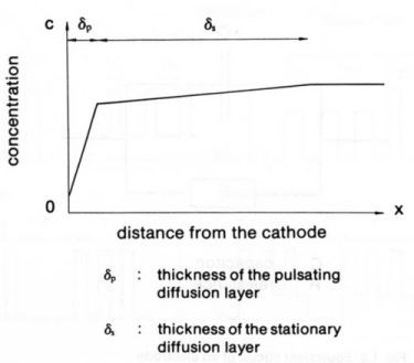
Figure 3 - Concentration profiles of the two diffusion layers in pulse electrolysis at the end of a pulse.
In the immediate vicinity of the cathode the concentration pulsates with the frequency of the pulsating current, decreasing during the pulses and relaxing in the interval between them. Thus, a pulsating diffusion layer exists close to the cathode. If the duration of the pulse is short, the diffusion layer does not have time to extend very far into the solution and in particular does not extend to the region where convection takes over the mass transport. Therefore, the metal deposited during the pulse must be transported from the bulk of the solution towards the pulsating diffusion layer by diffusion, which means that a concentration gradient also builds up into the bulk of the electrolyte. The thickness of this diffusion layer corresponds essentially to that which would be established under the same hydrodynamic conditions in DC electrolysis. Through this outer diffusion layer cations are also supplied towards the cathode during the off-time, and it is this supply that allows the relaxation of the pulsating diffusion layer during the off-time. The outer diffusion layer is essentially stationary.
The two distinct diffusion layers are related to two kinds of limitations. The depletion of the cationic concentration in the pulsating diffusion layer limits the pulse current density, and the depletion of the cationic concentration in the outer diffusion layer limits the average current density. Since the concentration gradient in the pulsating diffusion layer can be very high, increasing with shorter pulse length, the pulse current density can reach extremely high values, e.g., up to 10,000 times the usual DC values, without decrease of current efficiency because of hydrogen evolution. There is a quantitative relation between the maximum pulse duration as far as the current efficiency is concerned and the pulse current density. This maximum pulse duration is called the transition time. To sum up, the first limitation due to the mass transport effect in pulse plating is that the pulse duration should not exceed the transition time, while the second is that the maximum average current density cannot exceed the DC limiting current density. The latter is directly related to the establishment of the stationary diffusion layer. It is important to emphasize these deposition rate aspects in pulse plating because mistakes can be found in the literature, claiming that the average deposition rate can be very much increased as compared to DC. Cheh (1) and Ibl (2) have, in fact, demonstrated that the average current density in pulse plating cannot exceed the limiting current density in DC plating. However, Cheh (1) pointed out that the practical current density, which is below the diffusion limiting current density, can sometimes be increased in pulse plating as compared to DC while keeping a constant deposit quality. The increase, however, is only modest and does not represent the main advantage of the pulse plating technique, which rather consists in the improvement of deposit properties, which are related to the deposit structure.
4. Crystallization
The crystallization of the electrodeposited metal is a very important step of the electrogrowth since it influences directly the structure of the deposit and therefore its properties which represent the main interest for the user. The crystallization is the process by which the adatoms or adions incorporate in the crystal lattice. Crystallization (as schematically represented in Fig. 4) occurs either by the build-up of old crystals or the formation and growth of new ones. These two processes are in competition and can be influenced by different factors. High surface diffusion rates, low population of adatoms, and low overpotentials are factors enhancing the build-up of old crystals, while conversely low surface diffusion rates, high population of adatoms, and high overpotentials on the surface enhance the creation of new nuclei. In pulse plating, since the pulsed current density is usually considerably higher than the corresponding DC density, the population of adatoms on the surface during pulse deposition is higher than during DC deposition, resulting in an increased nucleation rate and there-fore in a finer grained structure. Grain refinement has quite often been observed by experimenters. Grain refinement in pulse plating is also favored by the enhancement of nucleation rates due to high overpotentials which result from high pulse current densities.
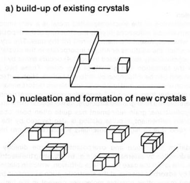
Figure 4 - Crystallization mechanisms.
While adatom population and overpotential can be directly influenced in a predictable direction by external factors, e.g., by adjusting the electrical parameters of the system, this is not the case for surface diffusion, which in plating baths is greatly influenced by adsorbed species at the electrode, such as organic brighteners, stress reducers and many other possible molecules present in the bath. The adsorption isotherm of these molecules is a function of the potential, and therefore by modulating the current, the nature of adsorbed species can continuously fluctuate. Depending on the adsorption and desorption rate constants, for given pulse parameters, adsorption or desorption of a species present in the electrolyte will influence surface diffusion in a different way than in DC, thus leading to different crystallization mechanisms and therefore to different physical properties of the deposit.
Another phenomenon that might occur in pulse plating during the off-period is recrystallization. Small grains are thermodynamically less stable than large ones because of high surface energy, and as in bubble coalescence, small grains tend to recrystallize. For this to occur, the surface should remain active during the off-time. Again, depending on different adsorbed species, the surface may be inhibited, in which case no recrystallization will occur, and the fine grains obtained during the on-time of electrolysis are stabilized.
One can think of using pulse plating to produce amorphous metals or alloys, for instance, from transition metals alloyed to metalloids. In pulse plating with very high pulse current densities, the concentration of adatoms at the interface is so high during the pulse that there is no time for ordering them into a crystal lattice, resulting in similar effects, as in rapid quenching.
5. Kinetics
In pulse plating, the electrodeposition rate can be considerably increased during the on-time as compared to DC. The kinetics of competitive reactions will therefore play a relevant role on the relative rate of possible competitive reactions, as in alloy plating or plating with hydrogen codeposition.
Referring to alloy deposition (see Fig. 5), if the slope of the polarization curve (I = f(E)) increases faster for the deposition of metal I than for metal II, the current efficiency for metal I will usually increase with increasing pulse current density. Similarly, in metal deposition accompanied by hydrogen evolution, if the slope of the polarization curve for metal deposition increases faster than for hydrogen evolution, the current efficiency for metal deposition will usually increase with increasing pulse current density.
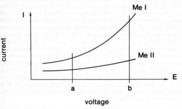
Figure 5 - Current-voltage curves for two competing reactions with different kinetics. An increase in voltage from a to b produces a change in current efficiency for reaction I (Me I) and reaction II (Me II).
However, particularly in pulse electrolysis with short pulses, adsorption and desorption effects can lead to unexpected trends in current efficiencies. For example, with hydrogen, which tends to desorb during the off-time, a given coulombic charge is consumed at the beginning of a new pulse in building up a new adsorbed layer of hydrogen. If the charge needed for this purpose represents a substantial part of the total charge of the pulse, the current efficiency for metal deposition can show a significant fall, even if the slope of the polarization curves would suggest an increase in current efficiency. This effect is illustrated in the case of gold deposition from a typical acid bath containing cobalt as a hardening additive (3,4).
Expected trends in current efficiency can also be vitiated by adsorption of metal species during the off-time. As an example, the deposition of rhenium can be mentioned. In rhenium deposition, rhenium is reduced from a heptavalent ion. Its reduction potential is much more negative than that of hydrogen ions, and thus the current efficiency for rhenium is usually very poor (less than 10 percent). Nevertheless, in pulse plating with very short pulses, the current efficiency increases up to 60 percent. The reason is that monovalent rhenium, the reduction potential of which is less negative than that of hydrogen, is adsorbed at the electrode during the off-time. If the on-time and pulse current density correspond approximately to the coulombic charge needed for the reduction of a Re-I monolayer, the current efficiency for rhenium is substantially increased. Adsorption during the off-time in this case thus results in a trend in current efficiency that would be quite unexpected according to considerations of steady state kinetics.
6. Pulsed current vs pulsed voltage
Electrolysis can be controlled by regulation of either current or voltage. In current regulation mode, the reaction rate is kept constant, and the potential varies as a function of time. In voltage regulation, the driving force for the reaction is kept constant and the reaction rate varies as a function of time. The advantages and disadvantages of these two modes of electrolysis are briefly discussed here for pulse plating. In current regulation, the average deposition rate can be very simply derived from the following equation:
[1]
while in voltage regulation the average deposition rate can be predicted only from computations of a speculative nature. The main advantage of voltage regulation is a better control of the current efficiency and of alloy composition. High overpotentials resulting from excessive concentration depletions are avoided. However, from a practical point of view, regulation of pulsed voltage is very difficult to achieve. To do it properly, a third electrode, a reference electrode, should be added to the system. Moreover, to get instantaneously a given potential at the electrode, the current should start theoretically from an infinite value, which is obviously not feasible because of apparatus limitations. On the other hand, at the end of a pulse, for instantaneous reestablishment of the starting potential (which might be the rest potential of the system), some metal should be redissolved; hence a constant voltage pulse requires a short inversion of current at the end of the pulse, which is not generally desirable. Furthermore, passivation may occur during the inversion. It should be pointed out that the above remarks apply to a regulated cathodic potential and not to the voltage between the negative and positive poles of the power supply. The latter is much easier to regulate, and sometimes, in particular for very high currents, the power supply engineer prefers it to the constant current regulation. For most applications, however, current regulation is preferred.
7. Pulse reverse
Among the different modes of current modulation, pulse reverse is a very early one and is very common. In early works, relatively long periods of forward and reverse cycles, longer than the usual on-time in pulse plating, were used. This kind of current is often called "periodic reverse." The term "pulse reverse" is not restricted to shorter cycles and applies to what is commonly understood under "periodic reverse" as well. The main purpose of inverting the current from cathodic to anodic during a short fraction of the total period is to remove metal preferentially from areas that tend to overplate during the cathodic part of the cycle. It is thus possible to considerably retard the development of dendrite formation or to improve the plating thick-ness distribution over complicated shapes. Changes in deposit structure, mainly grain size, can also be achieved because of forced nucleation at each new cathodic pulse. It is clear that adsorption-desorption as well as recrystallization phenomena will be quite different from those in pulse plating. It should be pointed out that pulse reverse is usually applied when the deposit is easily soluble in the electrolyte, otherwise passivation can occur. Sometimes, as in palladium deposition, the purpose of inverting the current is to remove codeposited hydrogen. In most cases the objective of the application of pulse reverse is to improve the plating thickness distribution.
From theoretical considerations the current distribution in pulse plating is often poorer than in DC. At least, an improvement as compared to DC normally cannot be expected. The deterioration of current distribution in pulse plating is due to higher ohmic drops in the solution, leading to higher current density differences between peaks and recesses of the substrate profile. Another reason for deterioration of current distribution in pulse plating is the decrease in activation overpotential with increasing current density. Activation overpotential is known for equalizing the current distribution (5). Deterioration of current distribution with pulse plating occurs if the pulse current density is substantially increased as compared to the normal DC density. If the pulse current density is the same as the usual DC density, pulse plating could even improve the current distribution. Because of divergent opinions reported in the literature regarding this matter, it seems important to underline the importance of the pulse current density.
Pulse reverse can be of great help in equalizing the plating thickness distribution. Areas exposed to concentrations of current density are preferentially plated in the cathodic cycle, but for the same reason, metal is preferentially removed in the anodic cycle.
To take full advantage of pulse reverse, the anodic current density should be adjustable independently of the cathodic current density. The reason for this is to increase the dissolution rate of peaks by applying very high anodic current densities, but for short time durations. It is obvious that the balance of electrical charges over a total period should remain cathodic. The manufacture of power supplies offering this capability involves complications, but this remains, nevertheless, an important requirement.
8. Other current modulations
Square-wave pulse plating and pulse reverse plating represent most of the applications today, while in the early days of pulse plating, because of less developed electronics, modified sine-wave pulses were used. Modern trends show increasing use of more sophisticated square-wave current modulations such as the ones represented in Fig.
In recent developments, improvements in physical properties of deposits have been observed by the use of a periodic reverse current mode with cycle times in the order of seconds, but with pulsing of current during both cathodic and anodic periods (pulsed pulse reverse). With optimization of electrical parameters, this approach offers a combination of the advantages of pulse plating with respect to modification of deposit structure and properties, with those of anodic deplating in improving the thickness distribution. The use of pulsed current allows a substantial increase in current density in both anodic and cathodic cycles. During the cathodic period this leads to grain refinement normally associated with pulse plating, which is further favored by the disturbance of growth steps by periodic inversion of the current. Thickness distribution is improved, not only by the normal anodic dissolution of metal from high spots or other exposed areas, but also because the preferential nature of this effect can be significantly enhanced by application of relatively short anodic pulses of high amplitude. Full advantage can be taken of this method only if all electrical parameters can be set independently, and in particular, if cathodic and anodic pulses can be independently regulated, e.g., with respect to pulse length and amplitude.
However, it should be kept clearly in mind that while in conventional pulse plating understanding has been gained based on theoretical models on the specific influence of the pulse parameters on-time, off-time and pulse current density, which enables pulse parameters to be set with due regard to the different physico-chemical phenomena involved, the introduction of more independent electrical parameters (at least ten as compared to three in conventional pulse plating) renders the optimal choice of parameters for expected trends in deposit properties much more difficult.
9. Early results in pulse plating
The publications on pulse plating issued before 1979 are summarized here. The works published after this date are more specifically treated in Theory and Practice of Pulse Plating as well as in the two Proceedings of AES Pulse Plating Symposia (6,7).
The use of modulated current in electrolysis is by no means new. The first application of periodically interrupted current dates back to the end of the 19th century, when it was used by Coehn (8) to produce coherent deposits of zinc. Baeyens (9) reviewed applications of various types of modulated current up to 1952, and Dini (10) has reviewed the main work carried out up to 1963 with reverse current, i.e., current comprising an anodic component in the interval between cathodic pulses. Studies on this subject have been covered by Cheh (11) and a review has also been given by Puippe, et al. (12).
The principal advantage of pulsed current is that it can be used to improve deposit properties. Advantages have also been claimed in respect to saving of time and reduction in energy requirements, but the former cannot be relied upon, and the latter is certainly not achievable.
Half-rectified alternating current somewhat resembles pulsed current, with the difference that the descending portion of the current curve is rounded instead of vertical. By using this type of current, Romanov (13) obtained compact deposits of zinc, free from dendrites, although, with continuous DC dendrite formation is inevitable. Gurovich and Krivtsov (14) also used this type of current in deposition of copper and zinc and found an increase in the number of grains, which they attributed to passivation of growth sites by adsorption of an inhibiting species during the off-time, thus forcing the formation of new nucleation centers for continued growth.
Decrease in crystallite size has often been observed (11,14-20), leading to a fine and more compact structure (21), and hence reducing the porosity of the deposit (16,22). Variations in pulsed current parameters also affect the dimensions of particles in the production of powder by electrolysis (23). Reduction in the internal stress of nickel deposits has also been recorded (24).
Not unnaturally, considerable attention has been directed to the effects of the pulsed current technique in gold plating, in view of the potential economic benefits that would accrue from improvements in properties. This aspect is of particular interest with respect to applications in the electronics industry, where annual global consumption of gold exceeds 100 tons (25). In this context Avila and Brown (17) have shown that it is possible by the use of pulsed current plating to increase the density and quality of gold coatings to an extent which permits a 50 percent reduction in thickness while maintaining the requisite conductivity of conductor patterns. Increase in ductility has been reported by Lendvay and Raub (26), while Reid (27) has shown that this method of electrolysis can eliminate nonmetallic inclusions in deposits from cobalt-harden-ed acid gold electrolytes (the so-called "polymer"), with substantial increases in density, ductility and conductivity of coatings. Reduced porosity has been observed by Mentone (28) and Rehrig (29), and other investigations concerning the effect of pulsed current parameters on the properties of gold coatings have been carried out by Angerer (3,30,31) and Bielinski (31).
Metals deposited by pulsed current exhibit smaller contents of adsorbed hydrogen than those produced with continuous current, as a result of desorption during the off-time (24,28,32). Since hardness is related to hydrogen content, the former is also affected. Leland (33), for example, deposited chromium with pulsed current, but with gradual reduction of the off-period during the course of electrolysis to finally approach continuous current conditions, and in this way obtained a coating in which both hydrogen content and hardness increased towards the outer layer.
Pulsed current has also been applied to alloy deposition (34,35,36), where it has been shown that the alloy composition approaches that of the electrolyte, providing a means of controlling the former, which is of particular importance in the deposition of colored alloys for decorative purposes.
Many workers have observed an increase in smoothness of deposits using pulsed current (13,14,37,38,39). Despic and Popov (40) found that surface roughness decreased with decreasing pulse length, which is attributable to mass transport phenomena. This effect has been investigated by other workers for copper (41-44), silver (41-42), and cadmium (45), the results obtained being explained in terms of a diffusional model developed by Ibl (46).
10. Concluding remarks
- It should be kept in mind that current "shaping" represents only one way of influencing a complicated system which contains many other dependent process parameters, such as electrolyte composition (concentration of electroactive ions, supporting electrolyte and additives), temperature, hydrodynamics and cell geometry. The interdependence of these process parameters with the pulse parameters should be at least qualitatively understood. One cannot expect that a given pulse shape will lead to the same deposit properties regardless of other process parameters. This fact could explain why sometimes contradictory observations are reported in the literature.
- Pulse plating, in allowing the use of simpler solutions and fewer additives, makes a useful contribution to the scientific basis of electroplating, and in this sense counters the "black art" reputation from which this general field still suffers to some extent.
- In order to set the electrical parameters, one has to remember the main limitations resulting from the charge and the discharge of the electrical double layer at the cathode interface and from mass transport effects. The on-time should be longer than the charging time of the electrical double layer and shorter than the transition time, the time at which the system starts working under limiting current conditions.
- The off-time between two pulses is not a "dead" time. Adsorption and desorption phenomena as well as recrystallization can occur.
- The main purposes of pulse plating are:
- the improvement of deposit properties, namely, porosity, ductility, hardness, electrical conductivity, wear resistance and roughness;
- deposition of alloys, the composition and structure of which are not obtainable with DC plating;
- improvement of plating thickness distribution by periodic inversion of polarity;
- increase in average deposition rate, although this can be achieved only to a rather limited extent.
References
1. H.Y. Cheh, Journal of the Electrochemical Society, 118 (4), 551 (1971).
2. N. Ibl, Metalloberfläche, 33, 51 (1979) and Surface Technology, 10, 81-104 (1980).
3. N. Ibl, J.CI. Puippe and H. Angerer, Surface Technology, 6, 287-300 (1978).
4. K. Hosokawa, H. Angerer, J.CI. Puippe and N. Ibl, Plating and Surface Finishing, 67 (10), 52-55 (1980).
5. N. Ibl, Comprehensive Treatise of Electrochemistry, Vol. VI, Chap. 4, E. Yeager, J.O'M. Bockris, B.E. Conway and S. Sarangapani, Eds.
6. Proceedings of the AES First International Pulse Plating Symposium, Boston, MA (April 19-20, 1979).
7. Proceedings of the AES Second International Pulse Plating Symposium, Rosemont, IL (Oct. 6-7, 1981).
8. A. Coehn, German Patent 75482 (1893).
9. P. Baeyens, Transactions Institute of Metal Finishing, 31, 429 (1954).
10. J.W. Dini, Metal Finishing, 61 (7), 52 (1963).
11. C.C. Wan, H.Y, Cheh and H.B. Linford, Plating, 61 (6), 559 (1974).
12. J.CI. Puippe, N. Ibl, H. Angerer and H.J. Schenk, Oberfläche-Surface, 20 (4), 77-85 (1979).
13. V.V. Romanov, Zhurnal Prikladnoi Khimii, 36 (5), 1050-1057 (1963).
14. R.I. Gurovich and A.K. Krivtsov, Zhurnal Prikladnoi Khimii, 41 (6), 1227 (1968).
15. A.P. Popkov, Journal Applied Chemistry USSR, 39, 1632 (1966).
16. M. Viswanathan and Ch.J. Raub, Galvanotechnik, 66 (4), 277 (1975).
17. A.J. Avila and M.J. Brown, Plating, 57 (11), 1105 (1970).
18. A. Hickling and H.P. Rothbaum, Transactions Institute of Metal Finishing, 34, 199 (1957).
19. A.M. Ozerov, N.P. Litvishko, I.N. Vavilina, P.M. Chetvertov and Y.E. Zhak, Zhurnal Prikladnoi Khimii, 40, 1144 (1967).
20. M. Viswanathan and Ch.J. Raub, Surface Technology, 4, 339 (1976).
21. W. Sullivan, Plating, 62 (2), 139 (1975).
22. K.I. Popov, D.N. Keca and B.I. Vuksanovic, Journal Applied Electrochemistry, 7, 185 (1977).
23. K.I. Popov, M.D. Maksimovic, M.G. Pavlovic and G.R. Ostojic, Journal Applied Electrochemistry, 7, 331 (1977).
24. W. Kleinekathofer and Ch.J. Raub, Surface Technology, 7, 23 (1978).
25. D. Lloyd-Jacob, Gold Bulletin, 4 (2), 25 (1971).
26. J. Lendvay and Ch.J. Raub, Metalloberfläche, 29 (4), 165 (1975).
27. F.H. Reid, Metalloberfläche, 30 (10), 453 (1976).
28. F. Mentone, Products Finishing (Cincinnati), 78 (April 1973).
29. D.L. Rehrig, Plating, 61 (1), 43 (1974).
30. H. Angerer, Dissertation 6213, ETH, Zurich (1978).
31. J. Bielinski, N. Ibl and H. Angerer, Oberfläche-Surface, 20 (1), 2 (1979).
32. C.L. Faust, G.R. Schaer and D.E. Sermones, Plating, 48, 605 (1961).
33. M. James Leland, "Programmable Pulse Electroplating Process," U.S. Patent 3,886,053 (cl. 204-36, C 23b), (May 27, 1975), Appl. 411.962.01 (Nov. 1973).
34. H. Leidheiser Jr. and A.R.P. Ghuman, Journal of the Electrochemical Society, 120, 484 (1973).
35. J. Winkler, German Patent 576585, cl. 48a (May 13, 1933).
36. R. Girard, Electrodeposition of Thin Magnetic Films, French Atomic Energy Commission, Grenoble Center of Nuclear Studies, (June 10,1965).
37. V.U. Polygraficky, British Patent 932,822 (1963).
38. N.P. Gnusin and Ya. Kovarski, Elektrokhim, 1, 46 (1965).
39. G. Savic-Maglic and A.R. Despic, Electrodeposition and Surface Treatment, 1, 429 (1972/73).
40. A.R. Despic and K.I. Popov, Journal Applied Electrochemistry, 1, 275 (1971).
41. M. Braun, Dissertation 5015, ETH, Zurich (1973).
42. N. Ibl and M. Braun, Chemie Ingenieur Technik, 45 (4), 182 (1973).
43. M. Braun and N. Ibl, Proceedings of the 8th Congress of the International Union for Electrodeposition and Surface Finishing, Basel (1972).
44. H.J. Schenk, Dissertation 5566, ETH, Zurich (1975).
45. J. Cl. Puippe, Dissertation 6225, ETH, Zurich (1978).
46. N. Ibl, Proceedings of "Surface 66", Basel, 48 (1966); Galvanotechnik + Oberflächenschutz, 7 (11), 256 (1966).
About the Editors of Theory and Practice of Pulse Plating

At the time of the book’s publication, Jean-Claude Puippe was R&D Manager for Werner Fluhmann AG, Dubendorf, Switzerland. He received his Ph.D. in 1978 from ETH in Zurich, where he worked under the direction of Dr. Norbert Ibl on pulse plating research. He worked on laser enhanced electroplating as an invited scientist at IBM. His fields of interest included alloy plating, difficult-to-plate metals and plating on plastics. He served the AESF as a member of the Research Board and was an Executive of the International Branch.
Today, he is Technical Director of Steiger Galvanotechnique SA, Lausanne, Vaud, Switzerland, where he has been employed since 1995. Although he is considered a pioneer in the field of pulse plating, over the years, he has applied is knowledge and experience to applied surface treatments electrochemical engineering for innovative industrial applications. His specialties include electroforming, surface treatment of titanium and advanced surface treatments. At Steiger Galvanotechnique, he is responsible for the innovation center of the company, dealing with electrochemical processes for the microfabrication, surface treatments of medical implants, for space and experimental physics applications. Besides his contributions to the AESF noted above, he is a member of the European Academy for Surface Treatments (EAST), and a member of the French Titanium Association. He was honored with the Pietro Cavalotti Pulse Plating Award (EAST) in 2018.

Frank Leaman received a Bachelor of Arts Degree in Chemistry from Eastern Mennonite University, Harrisonburg, Virginia. He completed graduate studies at Franklin and Marshall College, Lancaster, Pennsylvania. While working as a Chemist at Dentsply International, York, PA, Frank received a patent for the world’s first electroless platinum plating process. Later, he obtained several additional patents including the platinum coating of anodes having a polysulfone core. While employed by AMP, Inc. in Harrisburg, PA, Frank was responsible for the plating requirements of the Connector and Components Group. During this time, he received numerous cost reduction awards related to selective gold plating. He also conducted research on pulse plating of nickel, gold and palladium, and co-authored with Dr. Jean Claude Puippe, the world’s first textbook on pulse plating, Theory and Practice of Pulse Plating. In 1981, Frank became the owner and President of Electrochemical Company, Inc., a plating job shop that applied metallic coatings by electrolytic and electroless means to comply with specifications for military and aerospace applications. The company also specialized in gold and silver decorative plating. In 1992, Frank established Specialty Testing and Development Company, Inc. As CEO, he provides technical assistance and leads the firm in research and product development.
Related Content
A Chromium Plating Overview
An overview of decorative and hard chromium electroplating processes.
Read MorePossibilities From Electroplating 3D Printed Plastic Parts
Adding layers of nickel or copper to 3D printed polymer can impart desired properties such as electrical conductivity, EMI shielding, abrasion resistance and improved strength — approaching and even exceeding 3D printed metal, according to RePliForm.
Read MoreTroubleshooting Alkaline Zinc
One of the most common problems that can arise when plating with alkaline zinc is an imbalance of brightener in the solution. In this helpful Ask the Expert article, Chad Murphy of Columbia Chemical discusses how different zinc metal concentrations and brightener concentrations can impact efficiency.
Read MoreTrivalent Chrome Overview
As the finishing industry begins to move away from the use of hexavalent chromium to trivalent chromium, what factors should finishers consider as they make new investments? Mark Schario, chief technology officer for Columbia Chemical offers a helpful overview of this complicated topic.
Read MoreRead Next
Education Bringing Cleaning to Machining
Debuting new speakers and cleaning technology content during this half-day workshop co-located with IMTS 2024.
Read MoreDelivering Increased Benefits to Greenhouse Films
Baystar's Borstar technology is helping customers deliver better, more reliable production methods to greenhouse agriculture.
Read MoreEpisode 45: An Interview with Chandler Mancuso, MacDermid Envio Solutions
Chandler Mancuso, technical director with MacDermid Envio discusses updating your wastewater treatment system and implementing materials recycling solutions to increase efficiencies, control costs and reduce environmental impact.
Read More


