The Nucleation Dependent Growth Layer: A Structure Element in Electrocrystallization - The 10th William Blum Lecture
This paper is a re-publication of the 10th William Blum Lecture, presented at the 56th AES Annual Convention in Detroit, Michigan, on June 16, 1969.
by
Prof. Dr. Hellmuth Fischer
Recipient of the 1968 William Blum AES Scientific Achievement Award
Originally published as Plating, 56 (11), 1229-1233 (1968).
Editor’s Note: This paper is a re-publication of the 10th William Blum Lecture, presented at the 56th AES Annual Convention in Detroit, Michigan, on June 16, 1969. A printable PDF version is available by clicking HERE.
ABSTRACT
For the first time, it has been shown by Eichkorn that layer growth (not of growth-spirals) depends on continued nucleation of monoatomic layers building up growth layers. This has been done by determination of nucleation-overvoltage η and thickness of growth layers. During formation of growth layers, overvoltage must surpass η and time dependent adsorption of foreign substances must control the motion rate of monoatomic layers. Growth layers can develop to whiskers, columnar crystals, fiber textures, twinned or randomly dispersed structures.
The growth layer, a polyatomic macrostep, is a very important structure element for the construction of many polycrystalline aggregates of metal electrodeposits.
In general, we have to distinguish between two types of growth layers: self-perpetuating growth layers in spiral growth and nucleation-dependent growth layers.
Spiral growth layers do not need nucleation. They proceed from the penetration points of screw dislocations, which mostly are situated in the interior of crystal faces. The nucleation-dependent growth layers are generated at lattice faults preferentially situated at crystal or subcrystal boundaries, in the neighborhood of adsorbed foreign substances or at re-entrant grooves in twin formation.
The free energy for starting from a screw dislocation is much lower than that for formation of a nucleus. The nucleation work is decreased at lattice faults and may be further decreased by adsorbed foreign substances. Correspondingly, the overvoltage necessary for generation of a spiral growth layer is much lower than the nucleation overpotential.
Consequently, at overvoltages lower than the nucleation overvoltage, i.e., in the absence of strongly inhibiting adsorbates or with metals that are not sensitive to inhibition (e.g., like lead), electrodeposition occurs preferentially at screw dislocations forming self-perpetuating growth layers.
At overvoltages higher than the nucleation overvoltage, i.e., in presence of inhibiting adsorbates, growth layers will start by nucleation from the sites already mentioned. In these cases, the penetration points of screw dislocations may easily be blocked by inhibiting adsorbates.
As we shall see later, the nucleation-dependent growth layers may generate a very great variety of forms and aggregated structures. For that reason, our present knowledge of nucleation-dependent growth layers as a very important structure element for building up electrodeposits will be discussed in detail.
From extremely purified electrolytes neither growth spirals nor nucleation-dependent growth layers may develop, as Shanefield and Lighty1 have shown. The electrodeposits then grow by piling up atomic layers, but not growth layers. Growth layer formation needs the presence of adsorbable foreign substances, at least in traces.
If we assume that every growth layer consists of many crystal lattice planes and that every lattice plane is initiated by one two-dimensional nucleus, the thickness of the single growth layer must be proportional to the number of nucleation processes of the lattice planes building up the growth layer. Two years ago, my collaborator Eichkorn2 found that it is very likely that the growth layers develop by such continued nucleation. He showed this by x-ray analysis combined with a new method of measuring nucleation overpotentials.
The objectives of our investigation were electrodeposits of copper with the regular structure of the so called fiber-texture type. This type consists of compact aggregates of numerous crystal fibers all oriented perpendicular to the substrate ([220]-texture). Every fiber is composed of numerous growth layers situated one upon another. Such a structure may be produced by electrodeposition of copper from acid CuSO4 solution with an addition agent (o-phenanthroline). The mean size of the growth layers may be determined by x-ray analysis and thus it was possible to count the mean number, X of growth-layers deposited per cm2 and also, mentioned before, this number must be proportional to the rate, J2 of two-dimensional nucleation. For J2 the formula of Volmer is valid:
(1)
where C and Khkl, are constants, ηn2 is the overpotential necessary for two-dimensional nucleation, R is the gas constant and T the absolute temperature. Thus, substituting X for J2 in the Volmer equation, a linear relation between ln X and 1/ηn2 should prove that two dimensional nucleation is occurring during the formation of atomic layers as the constituents of the growth layers. Indeed this linear relation can be found as shown by Fig. 1. There ln X is plotted against 1/ηn2. The activation energy for the formation of a two-dimensional nucleus can be calculated from the slope. Thus for ηn2 equal to 10 mV, one finds an energy of 8 × 10-13 ergs. This value agrees well with the corresponding energy value for a nucleation of silver determined by Budevski3 in an entirely different way.
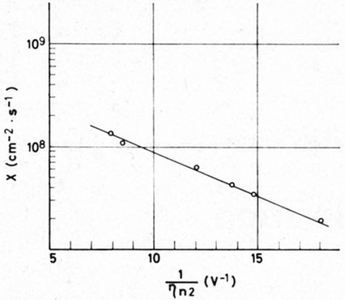
Figure 1 - Rate of the formation of growth layers (log X) vs the reciprocal overpotential of nucleation (deposition of copper in presence of o-phenanthroline).
The new method of obtaining ηn2 is based on a time-dependent separation of this overpotential from other kinds of overpotentials during electrolysis. This succeeds in transforming the deposit during electrolysis from a substrate-dependent structure which does not need a nucleation overpotential into the fiber-texture type developed by nucleation.
After switching on the current, copper is deposited on highly active copper. Continuing the numerous dislocations of the substrate, the deposit first originates without a nucleation overpotential. As Fig. 2 shows, at first only the overpotentials of resistance, charge-transfer and diffusion are measured.
When the value of η has attained a plateau, transformation into the fiber texture begins. Now in a S-shaped curve, ηn2 develops and attains a steady value, ηn2 can be directly measured. The calculated S-curve has been confirmed by experiment.
Now after having shown that growth layers of the non-spiral type very likely start by two-dimensional nucleation and claiming a nucleation overvoltage for this process, I will try to discuss the most probable mechanism of their growth. Still this must be done in a qualitative manner, for it is not yet possible to present a valid quantitative theory. A very simple and hence most appropriate objective in the research of the last ten years is the single platelet as the final form in the development of the growth layer. The deposited platelet and substrate are the same metal.
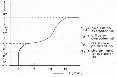
Figure 2 - Schematic curve of overpotential (η) versus time (t) with the single stages of overpotential during the deposition of copper in presence of an inhibitor (o-phenanthroline).
The experimental data upon which the model for the electrolytic growth layer is based have been gathered since 1924.
The mechanism of the growth of platelets and their aggregates may be divided into the following stages:
- Growth in height
- Lateral growth
- Ways of aggregation.
Growth in height
The first stage in the initial partial process of the layer growth is the generation of a two-dimensional nucleus, which grows out to a monoatomic layer. Consider the two cases A and B (Fig. 3) of electrodeposition of a metal from an electrolyte which was not highly purified. Suppose that the states of the surface of the substrate (in both cases the same densely packed face of a monocrystal) are entirely different for A and B. The figure shows schematic cross-sections of the metal plates consisting of the metal to be deposited which is considered the substrate in cases A and B. In the case of A, let the surface of the plate be a nearly ideal face without screw dislocations (for example as Budevski, et al.3 obtained by experiment); but in the case of B, let the face contain screw dislocations which are distributed statistically within the substrate. The dislocations should be covered with adsorbed impurity molecules. In case A, such active sites for adsorption are missing. In both cases the undisturbed densely packed face itself does not adsorb impurities which are present in the solution in a rather small concentration.
In both substrates, g indicates a cross section through a grain- or subgrain-boundary. In the case of A, this boundary is practically undisturbed, whereas it is strongly disturbed in B. Consequently, a molecule of an impurity f may have been adsorbed in B at the re-entrant edge formed by g and the substrate plane.
Now in both cases A and B, the previously mentioned two-dimensional nucleus n should be generated. In case A, it will be generated preferentially at the re-entrant edge formed by the boundary g and the substrate plane, in case B at the re-entrant edge formed by the molecule f which is adsorbed in contact with g. The molecule should rise to some height above the nucleus. The nuclei in both A and B begin to grow out to a monoatomic layer spreading over the substrate face.
During lateral outgrowth, the atomic layer of case A does not encounter any obstacle. On the other hand the layer in the case of B continuously meets impurity molecules adsorbed preferentially on screw dislocations. The out-growing metal layer incorporates the molecules. The adsorbates can hardly escape from this fate by desorption, because their incorporation takes place very quickly since the current density at the edge e of the layer, the unique site for an incorporation of discharged metal ions, is very high. But the atomic layer cannot bury the molecules completely, since, as already mentioned, they will be larger than the metal atoms.
Furthermore, the free energy ΔG*hkl of forming a stabilized two-dimensional nucleus on the substrate face will be different in cases A and B. There is the (somewhat simplified) formula which is valid for one mole:
(2)
where is the specific edge free energy, a is a constant, z is the valence of the metal ion, and F the Faraday constant. In case B, the adsorption of impurities on g may decrease and increase ηn2. Both effects will decrease ∆G*hkl.
In case B (Fig. 3) the nucleation frequency will increase substantially because of the easier nucleation compared to case A. In other words, during the time for stabilizing nucleus in A, many stabilized nuclei will form consecutively in B. This faster production of nuclei in B depends on two conditions: first, every nucleus as it forms will be in contact with an adsorbed molecule of an impurity, and secondly, before entering every new stage or nucleation the overvoltage must reach once more the nucleation overvoltage ηn2 which is now increased because of adsorption of impurities.
It is not difficult to imagine the first condition. The second nucleus can readily form at a re-entrant edge formed by the upper face of the first nucleus and by the free edge face with which the molecule of impurity f towers above the nucleus (Fig. 3). On the other hand the second nucleus will tower now above the molecule f.
This induced preferred adsorption of a new impurity molecule f ' now in its turn facilitates the formation of a third nucleus. Thus, by further continued adsorption of foreign molecules one above another, the fourth, fifth, etc. nucleus will develop in a rapid sequence determined by the adsorption rate of the foreign molecule. Continued nucleation will occur, provided that the second condition now to be discussed is fulfilled.
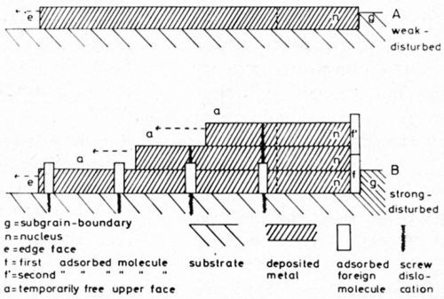
Figure 3 - Nucleation and outgrowth of atomic layers (A on a substrate free from screw dislocations and adsorbed molecules, B on a substrate with screw dislocations and adsorbed molecules).
How will the overvoltage η reach and surpass the nucleation overvoltage ηn2? As already mentioned, the current density of metal deposition on the edge e of the atomic layer will be very high. Initially it could have a theoretical value surpassing the limiting current density of metal deposition by several orders of magnitude. When initially it has to adapt to this limiting current density, the corresponding diffusion overvoltage ηd must considerably exceed the nucleation overvoltage ηn2.
Hence, the second nucleus will be formed very quickly and, after the second nucleation, the second atomic layer will move over the first. Since the edge regions now are doubled, correspondingly the edge current density should be halved. But theoretically, it would be still far higher than the limiting current density to which it must adapt itself again. The same should apply to a still further addition of edge regions of a series of subsequent atomic layers moving one over the other. In other words, the current density at the sum of their edge regions would remain approximately at the value of the limiting current density and in every case almost at the same overvoltage ηd. Hence ηd would continue to exceed considerably the nucleation overvoltage ηn2.
But during the further formation of atomic layers, the edge current density following the permanent increase of the edge face (the sum of the single layer edges) should drop continuously to values lower than the limiting current density. Nevertheless, the prevalent diffusion overvoltage ηd should remain higher than the nucleation overvoltage ηn2. Thus still many nuclei should form one after another, and the same number of atomic layers grow one over the other. There may be, depending on the value of nucleation overvoltage, several hundred or perhaps several thousand such layers.
As reaching the corresponding maximum value of the diffusion overvoltage depends on time, and the time necessary for it will increase with the drop of the edge current density, the nucleation frequency must gradually decrease. Consequently, atomic layers will form less frequently. But, when finally the overvoltage during electrolysis is less than the nucleation overvoltage, nucleation and the succeeding outgrowth of layers must cease entirely.
Now the fundamental question to be interpreted is how one polyatomic macrostep will arise from the many atomic layers. This process which accompanies nucleation and outgrowth depends, as already mentioned, on the effect of adsorbed foreign substances. Where is such effect localized and how is it manifested? As we have assumed, during the outgrowth of the first atomic layer, adsorption of foreign molecules has taken place on the subgrain boundary g and on dislocations in the substrate face (Fig. 3).
But, during the first sequence of atomic layer formation, foreign substances will be rarely adsorbed at their edges because of the high current density, which still is prevalent there. In this stage, the time necessary for covering the edges with foreign substances still would be too short. Substances which are adsorbed there would be quickly incorporated into the deposited metal. Likewise adsorbates will not yet cover the surface planes a (Fig. 3), which initially may exist only for a very short time, because all these surface planes will be covered very rapidly by the following layer. Thus, initially, only the adsorbates on the substrate face and in the subgrain boundary may interfere with the described growth mechanism.
The molecules adsorbed on the substrate face will be buried quickly by the first atomic layer (Fig. 3, B). But since, during this process, they will partly cover the edge of the layer, metal atoms may deposit during this coverage only on free parts of the edge. On the other hand, the succeeding second layer will attach itself only to the parts of the foreign molecules raised above the first layer. These parts will cover the edge of the second layer to lesser degree than the molecules did with the first. Thus, the second layer will move faster than the first and will overtake the first. Likewise, the third and fourth layers will overtake the preceding ones. All layers will then unite to a macrostep (Fig. 4).
But in the course of further growth (Fig. 4) time-dependent adsorption will arise, at first on dislocations of the "oldest" face-segments e.g., a1, a2 between the steps (close to the edge of the preceding step), then on the edge face em of the macro-step and finally at the "oldest" edges of atomic layers, e.g., e1, e2.
All these adsorbates situated in different positions will result in the same effect: The greater part of current now will be directed to yet uncovered re-entrant edges of "younger" layers so that these may overtake the "older" too. Thus all layers will be "bunched" to the growth layer. This layer finally obtains its definitive thickness, when nucleation has ceased.
I presented basic ideas of this interpretation in 1948.4 Frank proposed in 1949 the conception of the "bunching effect" as the characteristic principle of uniting many atomic layers to growth layers.5 This bunching effect, which depends on mobile or immobile adsorbed foreign substances, is observed by no means only in electrocrystallization, but also in most other crystallization processes.
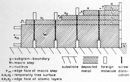
Figure 4 - Subsequent nucleation, outgrowth and "bunching" of atomic layers forming a macrostep.
Lateral growth
While the height of the growth layer increases by bunching, it grows in the lateral direction also. The layer which has started, as already mentioned, from a foreign molecule adsorbed at a grain boundary (or otherwise, in the case of denser coverage at a covered dislocation) can grow very regularly in three directions and in height and finally becomes a platelet (Fig. 5). The edge faces will be rather rounded.
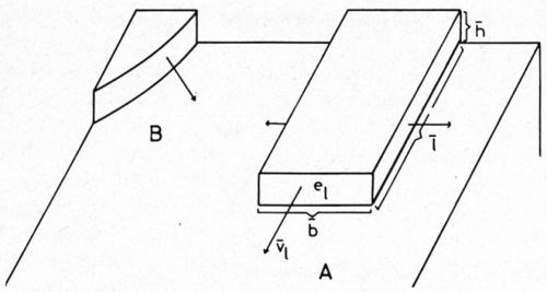
Figure 5 - Regular (A) and random (B) growth of a growth layer.
On the other hand, the growth layer may sometimes prefer to grow randomly, e.g., rather towards one side and in height. The effect of the substrate is that layer growth occurs only on the most densely packed planes.
In a model of regular growth (Fig. 5), let h be the thickness, l the length and b the width. If ̅ν1 is the mean rate of the growth in length, then ̅ν1 will be proportional to the current density i, on the edge face e1. Consequently,
(3)
Here, l̅ , h̅ and b̅ are the average values, t is the time of layer moving, J the total current, which is being kept constant. As long as h̅ and b̅ are increasing with t, ir resp. ̅ν1 must decrease correspondingly. Many authors6 have confirmed that growth layer moving tends to slow down on the substrate. Consequently, at different times, one will observe entirely different ̅ν1 values. It has been repeatedly confirmed too, that ̅ν1 changes inversely with h̅ . h̅ and l̅ are approximately proportional to √t̅, as Howes7 found 1959, when he deposited copper cathodically as platelets on (l00)-copper (sliced from mono-crystal) from acid solution of copper sulfate (not highly purified), h̅ = K√t̅ controls l̅ = K'√t̅ (K and K' are constants.) if the layer grows regularly and b̅ remains constant (in the case of lateral contact of the growth layer with the neighboring ones).
By substituting h̅ in eq (3) for K√t̅ one obtains:
(4)
where C is a proportionality constant. That means:
(5)
Probably the √t̅ relation is connected with the time-dependent drop of the edge current density and the increase of the adsorption of foreign substances close to the nucleus, so that the nucleation overvoltage ηn temporally increases too dependent on time. This rise of ηn likewise decreases the nucleation frequency.
In extremely purified electrolyte solutions, the t relation obviously is no longer valid, as Damjanovic, et al.8 have found. This seems to be connected with the phenomenon of the so-called "fading out" of growth layers, which occurs in extremely pure solutions. Fading out means a spontaneous "debunching" of the macrosteps into microsteps. Therefore, in this special case, the dimensions of the growth layers and their rate of moving will be influenced by the fading out occurring simultaneously with growth.
Fading out is demonstrated schematically by Fig. 6.9 Let XX', YY' and ZZ' be the cross-sections through the same surface region at different times. The macrostep in the center in XX' has debunched in the subsequent time (YY') into a series of microsteps. In the subsequent third time (ZZ'), the debunching process has still further continued.
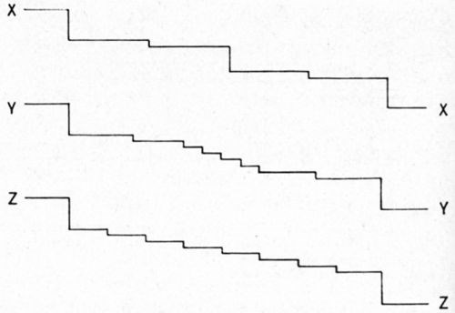
Figure 6 - Model for fading out of a macrostep from its end. (After Bockris and Razumney9).
Damjanovic, et al.8 have assumed the debunching effect to be caused by adsorption of foreign substances from the edge face of the macrostep. This desorption may become possible when the growth layer grows into a site of the electrolyte where locally the concentration of adsorbable impurities has been preferentially consumed from the solution. As a consequence of this local desorption, potential differences between neighboring growth layers may occur whereby local cathodes and anodes must become effective. Then the anodic parts of the growth layers break up into microsteps. Fading out can be hindered if one adds traces of inhibiting substances to the extremely purified electrolyte or if one uses less purified solutions.
Let us now return to these not extremely purified electrolytes. As Kohlschuetter and Toricelli10 observed already in 1932, the step heights of the growth layers vary on substrates of different orientation between 10-6 and 10-3 cm; the rates of lateral propagation between 10-2 and 10-4 cm/sec. In extremely purified solutions, Damjanovic, et al.8 have found the abnormal rate of 10-6 cm/sec. The great deviation of this value from those of others may have at least two different causes. First Damjanovic, et al. have observed that in extremely purified electrolytes the major part of the electrodeposit grows without bunching of the atomic layers, i.e., in the same manner as Shanefield and Lighty1 have shown with their electrolytes which seem to be even purer than the electrolyte of Damjanovic, et al. In any case, these authors have found that their rate values observed by experiment were 20 times smaller than the calculated ones. Secondly, the higher rate values of Kohlschuetter and Toricelli10 obviously are found in an initial stage of layer growth, whereas the values of Damjanovic are observed in a later one.
Since 1961, several authors tried to develop a quantitative theory of the bunching effect in the formation of growth layers by electrodeposition.11 But even today, theory and experiment do not yet agree satisfactorily. One reason for this deficiency may be the imperfection of the measurement. The interferometric methods do not allow for a determination of the size and motion rates of atomic layers before bunching to become growth layers.
On the other hand, even the model calculated by Bertocci12 in 1968, which perhaps is closer to reality than other models, seems to be oversimplified. This model does take account of time-dependent adsorption and of overvoltage. But Bertocci assumes, e.g., a symmetrical distribution of the adsorbed substances on the layer surface and an immobility of these substances. On the other hand, he does not take account of incorporation of adsorbates and assumes only one sort of overvoltage, the charge-transfer overvoltage. As we have just seen other overvoltages, e.g., that of diffusion which is time-dependent, and that of nucleation, obviously play an important role.
Ways of aggregation
If growth layers grow laterally, they should finally meet the neighboring growth layers spreading in the opposite direction across the surface. When this occurs, growth layers with small coverage of foreign substances on their side faces then may merge completely without leaving grooves.7,13 By this merging process, well-developed crystal platelets arise, the mosaic structure of which cannot be recognized under the light microscope. When the coverage with adsorbed foreign substances of the original boundaries of the single macro-steps which are growing together is poor, the adsorbates obviously will be incorporated. This complete merging is observed, e.g., with metals which are not very sensitive to inhibitors, such as lead, silver or copper, deposited from acid solutions without addition agents. Platelets in the merged form often have a diameter of about 200-500 microns.
If the edge faces are covered more densely with foreign substances, the macrosteps merge incompletely or they do not merge at all. In the case of great differences in height of merging macrosteps, a remnant step may remain after growing together.
As we have seen, lateral growth of a single growth layer must cease first, when this layer contacts neighboring growth layers or second, when the incorporation of metal ions at the edge face of the layer is stopped by adsorbed foreign substances blocking the edge face almost completely. In these cases, continued metal deposition, at least on the surface of this growth layer, is only possible by repeated two-dimensional nucleation starting on the upper face of the growth layer. This upper face is densely packed and oriented like the substrate face. During a period of rest after the final height of the growth layer had been reached, the crystal imperfections situated on this face could be covered preferentially by adsorbed foreign substances. These adsorbates, e.g., on the subgrain boundaries, probably cause the rise of overvoltage necessary for again exceeding the nucleation overvoltage.
Thus, a first new two-dimensional nucleus again will be developed followed by many others. A new growth layer then will arise there as before, passing through the same stages of bunching, growing in height and spreading laterally over the first growth layer.
Continuing in this manner by piling up many growth layers one above the other and eventually by lateral merging (if the coverage of the edge faces with adsorbed foreign substances is not too high), a great variety of aggregated structures may be built up. Figure 7 shows an etched cross-section of copper electrodeposited from an acid CuSO4 solution (not highly purified) at room temperature in the form of the so called basis oriented reproduction type (BR). This photomicrograph reveals very clearly the growth layers piled up one above another in the different crystallites. Probably the considerable width of these layers is caused by merging of layers which were narrower.
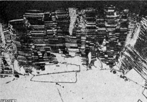
Figure 7 - Cross section of the BR-type (Cu deposited from acid CuSO4 solution, magnification 250×).
In Fig. 8 an etched cross-section of copper is shown which has been electrodeposited at room temperature from an acid CuSO4 solution containing 5 × 10⁻⁴ mol/L β-naphthoquinoline as an inhibiting addition agent. The copper deposit has the structure of the already mentioned fiber-texture type (FT). In this case, a great part of the substrate face is covered by inhibitor molecules in a nearly statistical distribution. Two-dimensional nuclei may be formed leaning against an adsorbed inhibitor molecule and growing out to an atomic layer. Thus, the density per cm2 of nuclei and of growth layers formed by bunching must be much higher than in the case of the BR-type. Consequently, the single growth layers have a very narrow width. The strong adsorption of foreign substances on the edge faces of the growth layers hinders in any case the merging of layers. Hence, the FT-type has a rather regular structure consisting, as already mentioned, of numerous fine fibers oriented perpendicular to the substrate. Every fiber is subdivided into numerous growth layers piled up one above the other.
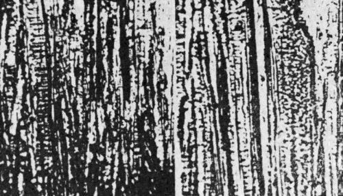
Figure 8 - Cross section of the FT-type (copper deposited from acid CuSO4 solution + 5 × 10⁻⁴ mol/L β-naphtoquinoline, magnification 1200×).
In Fig. 9 is seen the cross-section of copper with growth layers piled up in a twin position [the so-called twinned transition type (TT)]. The copper has been electrodeposited at room temperature from an acid CuSO4 solution containing 5 × 10⁻³ mol/L acridine. The growth layers likewise arise by bunching of atomic layers. The condition for twinning is the presence of re-entrant grooves. There the two-dimensional twin-nuclei are formed. They grow out in a definite angle to two atomic layers towards the opposite directions of the defined twin-orientation. Before new nucleation arises the re-entrant groove has been renewed by the twin growth of the two preceding growth layers.
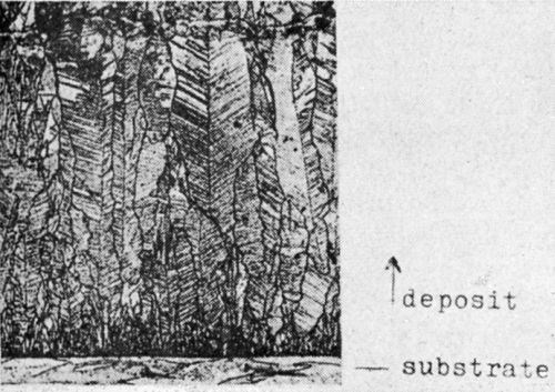
Figure 9 - Cross section of the TT-type (copper deposited from acid CuSO4 solution + 5 × 10⁻³ mol/L acridine, magnification 600×).
As Pangarov14 has shown, the work for two-dimensional twin-nucleation does not differ very much from that of normal two-dimensional nucleation. It is still an open question why just twin nuclei arise instead of normal ones.
Probably twinning depends on the structure and orientation of the substrate and on the species of adsorbed foreign substances. But on the other hand, some of these substances may suppress twinning by blocking of re-entrant grooves. Therefore, the twinned orientation of growth layers occurs mostly as a transition form between BR-type and FT-type.
Summary
Summarizing my lecture, I must underline that it is the adsorption of impurities or of added foreign substances which causes the great variety of structures in the electrodeposition of metals. Adsorbed foreign substances promote the formation of growth layers by inciting nucleation and bunching. The variety of structures arises by the merging and aggregation of growth layers, the size of which depends on the degree of local coverage with adsorbed substances.
References
1. D. Shanefield and P.E. Lighty, J. Electrochem. Soc., 110, 973 (1963).
2. G. Eichkorn and H. Fischer, Z. Phys. Chem. NF, 53, 29 (1967).
3. E. Budevski, W. Bostanoff, T. Witanoff, Z. Stoinoff, A. Kotzeva and R. Kaischew, Electrochim. Acta, 11, 1697 (1966).
4. H. Fischer, Z. Metallk., 39, 204 (1948).
5. W.K. Burton, N. Cabrera and F.C. Frank, Nature (London), 163, 398 (1949).
6. V. Kohlschuetter and A. Torricelli, Z. Elektrochem., 38, 213 (1932).
Th. Erdey-Gruz, Z. Phys. Chem. (A), 172, 157 (1935).
K. M. Gorbunova, Bull Acad. Soc. USSR, 1175 (1938).
V. R. Howes, Proc. Physical Soc. (London), 74, 616, 618 (1959).
H. Fischer, Electrochim. Acta, 2, 50, 79, 144 (1960).
7. V.R. Howes, Proc. Physical Soc. (London), 74, 616 (1959).
8. A. Damjanovic, T.H.V. Setty and J.O'M. Bockris, J. Electrochem. Soc, 113, 429 (1966).
A. Damjanovic, M. Paunovic and J.O'M. Bockris, J. Electroanalytical Chem., 9, 94 (1965).
9. J.O'M. Bockris and G.A. Razumney, Fundamental Aspects of Electrocrystallization, Plenum Press, New York, 1967; p. 106.
10. V. Kohlschuetter and A. Torricelli, Z. Elektrochem., 38, 213 (1932).
11. N. Cabrera in: Reactivity of Solids, Elsevier, Amsterdam, 1961; p. 345.
W.W. Mullins and J.P. Hirth, J. Phys. Chem. Solids, 24, 1391 (1963).
U. Bertocci, Electrochim. Acta, 11, 1261 (1966).
L.D. Hulett and F.W. Young Jr., J. Electrochem. Soc., 113, 410 (1966).
12. U. Bertocci, Surface Science, 9, 18 (1968).
13. G. Wranglen, Electrochim. Acta, 2, 130 (1960).
14. N.A. Pangarov, Phys. Stat. Sol., 20, 371 (1967).
About the author

In 1950, Dr. Fischer became Professor of Electrochemistry at the Technische Hochschule Karlsruhe, and in 1960 he was promoted to Full Professorship and director of the Lehrstuhl fur Electrochemie. This school trained the largest number of electrochemists of any school in Europe. Between 1950 and 1960, he was also director of chemical laboratories of Siemens and Halske AG in Munich.
Professor Fischer published over 100 papers in the areas of the morphology of electrodeposits, the influence of inorganic and organic inhibitors on electrocrystallization, and the nature of corrosion of metals. His best known work, the book Elektrolytische Abscheidung und Elektrokristallization von Metallen, is considered by many workers in the field of electrodeposition to be the most definitive one of its kind. It has contributed much to the understanding of how addition agents influence the deposition of metals.
In the area of professional societies, he was active in the Bunsengesellschaft, an honorary member of the Societe de Chimie Industrielle, and was a Vice-President and President of the Comite International de Thermodynamique et de Cinetique Electrochemiques (CITCE). In 1957 he became Chairman of the CITCE Commission on Corrosion.
Professor Fischer was much in demand as a participant in international meetings devoted to electrodeposition and corrosion because of his lucid method of lecturing and his stimulating leadership in the art of discussion. He was one of three lecturers at Interfinish '68 in Hanover. In the United States, he participated in meetings of The Electrochemical Society and the Gordon Research Conference on Electrodeposition.
Dr. Fischer was interested in the many branches of art - in particular art of the 19th and early 20th centuries, and in music from Brahms to Bartok, in painting from Renoir to Kokoschka, in sculpture from Rodin to Henry Moore. His special hobby was German literature of that time and German style of writing.
He was married and had two sons. The elder son was an Assistant Professor of theoretical chemistry at Technische Hochschule in Munich. In 1967, the younger was finishing a doctor's thesis on organic chemistry at the University of Heidelberg.
Related Content
Curing Oven Basics
Simply heating up the substrate does not cure the coating. There are many variables to consider when choosing the best cure oven for your application...
Read MoreConveyors and Paint Systems
Choosing the right conveyor system, coating technology, and ancillary equipment.
Read MoreTop Reasons to Switch to a Better Cleaning Fluid
Venesia Hurtubise from MicroCare says switching to the new modern cleaning fluids will have a positive impact on your cleaning process.
Read MoreUnderstanding and Managing White Spots on Anodized Aluminum
Having trouble with spotting defects when anodizing? Taj Patel of Techevon LLC offers a helpful overview of the various causes of white spots and potential solutions.
Read MoreRead Next
Education Bringing Cleaning to Machining
Debuting new speakers and cleaning technology content during this half-day workshop co-located with IMTS 2024.
Read MoreDelivering Increased Benefits to Greenhouse Films
Baystar's Borstar technology is helping customers deliver better, more reliable production methods to greenhouse agriculture.
Read MoreEpisode 45: An Interview with Chandler Mancuso, MacDermid Envio Solutions
Chandler Mancuso, technical director with MacDermid Envio discusses updating your wastewater treatment system and implementing materials recycling solutions to increase efficiencies, control costs and reduce environmental impact.
Read More



.jpg;maxWidth=300;quality=90)


